Factory Direct High-Purity Quartz & Optical Components
Manufactured in Donghai County—the epicenter of global quartz purification—our components deliver sub-nanometer surface precision, unmatched thermal stability, and deep ultraviolet clarity with 1-piece custom prototyping.
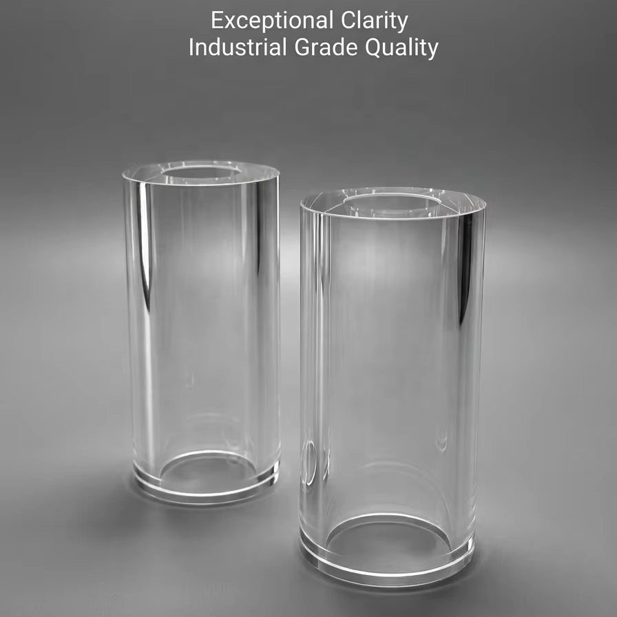
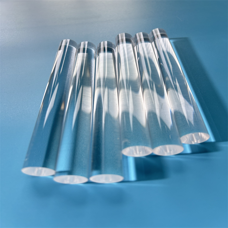
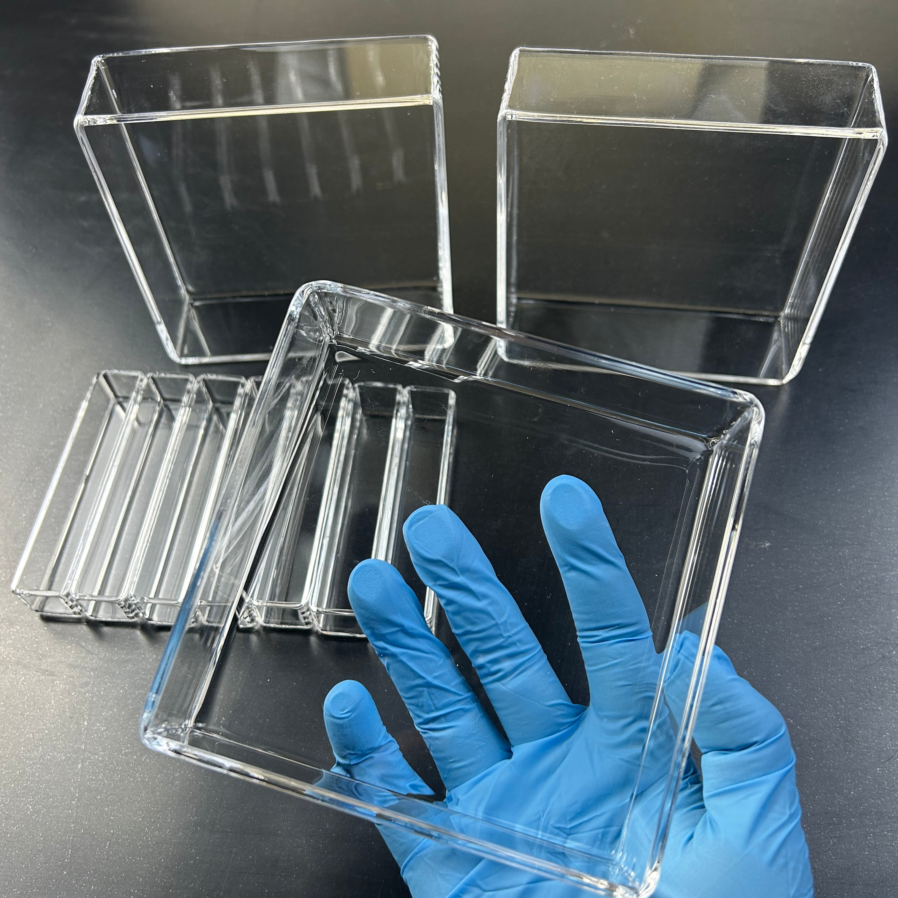
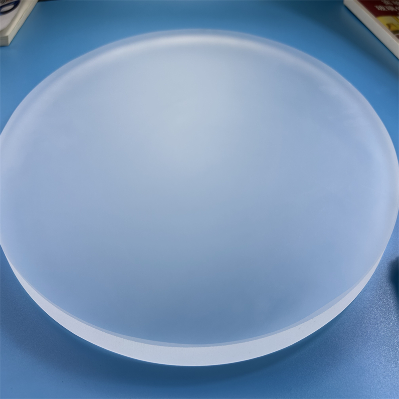
Engineering Physics: Fused Silica vs. Fused Quartz Optical Lenses
Understanding spectral transmittance, hydroxyl ion [OH⁻] absorption bands, and laser-induced damage thresholds (LIDT) for CE compliance in European machinery.
When procurement managers, laser system architects, and semiconductor equipment engineers evaluate optical lenses, windows, and light guides, confusion frequently arises between natural fused quartz and synthetic fused silica. While both are colloquially referenced as "quartz glass," their micro-structural morphology, trace impurity profile, and photochemical characteristics diverge dramatically under deep-ultraviolet (DUV), high-energy laser irradiation, and severe thermal cycles.
1. Spectral Transmission and Chemical Homogeneity Bands
Natural optical fused quartz—synthesized by electric-arc or gas-fusion melting of ultra-pure natural Donghai quartz crystals (SiO₂ ≥ 99.99%)—exhibits remarkable structural integrity and resistance against devitrification. However, metallic trace contaminants such as Aluminum (Al ≤ 15-20 ppm), Titanium (Ti ≤ 1.5 ppm), and Iron (Fe ≤ 0.8 ppm) create shallow absorption traps in the DUV band (185 nm – 260 nm). Consequently, natural quartz grades such as JGS2 or JGS3 are optimally deployed for visible (VIS), near-infrared (NIR), high-temperature viewing ports, and semiconductor chemical vapor deposition (CVD) environments.
Conversely, synthetic fused silica (optical grade JGS1 / equivalent to Suprasil or Corning 7980) is synthesized via chemical vapor deposition (CVD) through the flame hydrolysis of silicon tetrachloride (SiCl₄). This gas-phase synthesis limits total metallic impurities to sub-ppb levels, yielding near-unity internal transmittance down to 185 nm without solarization under 193 nm ArF excimer or 266 nm/355 nm Nd:YAG third/fourth-harmonic laser irradiation.
Crucial Procurement Takeaway for Engineers: If your system operates within the deep UV (185–260 nm) or requires laser damage threshold exceeding 10 J/cm² at 1064 nm (10 ns pulse), specify JGS1 Synthetic Fused Silica. For thermal process tubes, furnace sight glasses, and photolithography stages operating between 300 nm and 2100 nm, high-purity natural fused quartz (JGS2) provides identical mechanical and thermal benefits at 40% lower substrate procurement costs.
2. Material Property Benchmark: Fused Quartz vs. Optical Crown Glass
Optical quartz possesses an exceptionally low coefficient of thermal expansion (CTE) of 5.5 × 10⁻⁷ /K, nearly twenty times lower than standard borosilicate or optical crown glass (such as N-BK7). This near-zero expansion eliminates thermal blooming, optical wavefront deformation, and catastrophic thermal fracture under steep thermal gradients.
| Physical / Optical Parameter | JGS1 Synthetic Silica | JGS2 Optical Fused Quartz | Standard Optical Glass (N-BK7) | Procurement Relevance |
|---|---|---|---|---|
| Usable Transmission Range | 185 nm – 2500 nm | 220 nm – 2500 nm | 350 nm – 2000 nm | Determines DUV vs. NIR applicability |
| SiO₂ Purity Level | ≥ 99.9999% (Electronic Grade) | ≥ 99.99% (Donghai Natural) | Multi-component silicates | Controls laser degradation & solarization |
| Hydroxyl [OH⁻] Content | High-OH (800–1200 ppm) / Low-OH <1 ppm | < 30 ppm typical | N/A | Eliminates 2.73 μm infrared water bands |
| Thermal Expansion (CTE) | 5.5 × 10⁻⁷ /K (0–300°C) | 5.5 × 10⁻⁷ /K (0–300°C) | 7.1 × 10⁻⁶ /K | Guarantees wavefront stability under laser heat |
| Thermal Shock Resistance (ΔT) | > 1100°C to water plunge | > 1000°C to water plunge | ≈ 120°C fracture point | Prevents field failure during furnace cycles |
| Softening Point | 1683°C | 1680°C | 710°C | Enables prolonged exposure in semiconductor CVD |
| Laser Damage (LIDT @ 1064nm, 10ns) | > 15 – 25 J/cm² | > 8 – 12 J/cm² | < 5 J/cm² | Critical metric for multi-kilowatt fiber lasers |
| Abbe Number (vd) | 67.8 (Low dispersion) | 67.8 | 64.17 | Minimizes chromatic aberration across bands |
Enterprise Strengths: Lianyungang Zelvo Quartz Products Co., Ltd.
Combining Donghai County's localized raw-material purification cluster with aerospace-level computer numerically controlled (CNC) grinding, diamond core-drilling, and ISO cleanroom inspection.
Donghai Cluster Integration
Located in China's "Crystal Capital," Zelvo Quartz controls raw silicon ingot selection directly from primary refining furnaces, guaranteeing authentic 99.99% SiO₂ baseline purity without intermediary trader markups.
Micro-Machining & Laser Milling
Our workshop integrates 5-axis CNC machining centers, high-speed diamond slicing, CO₂ laser hole-drilling down to 0.2 mm diameters, and precision edge bevelling compliant with DIN ISO 10110 standards.
Flame Working Mastery
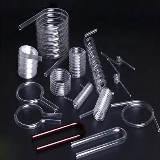
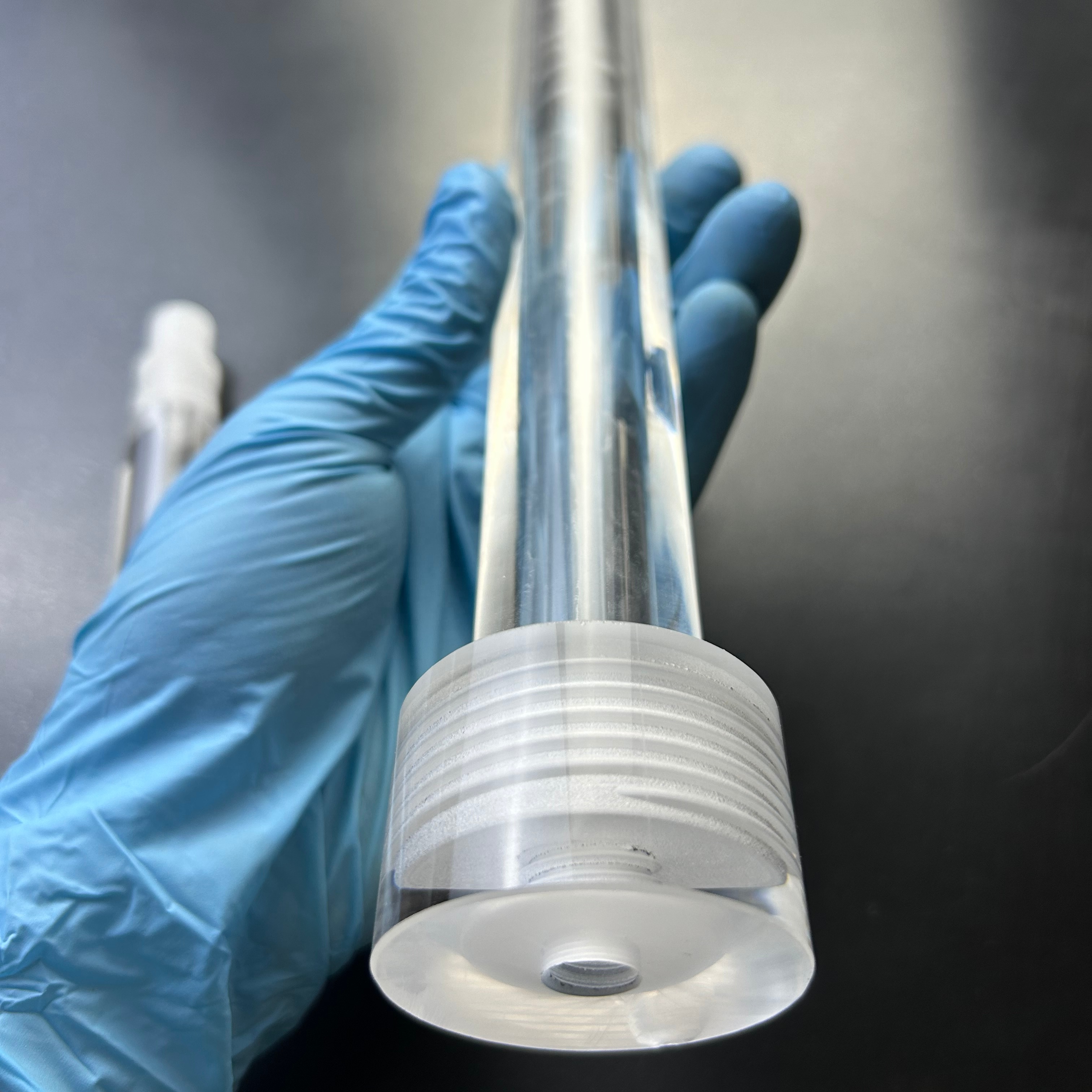
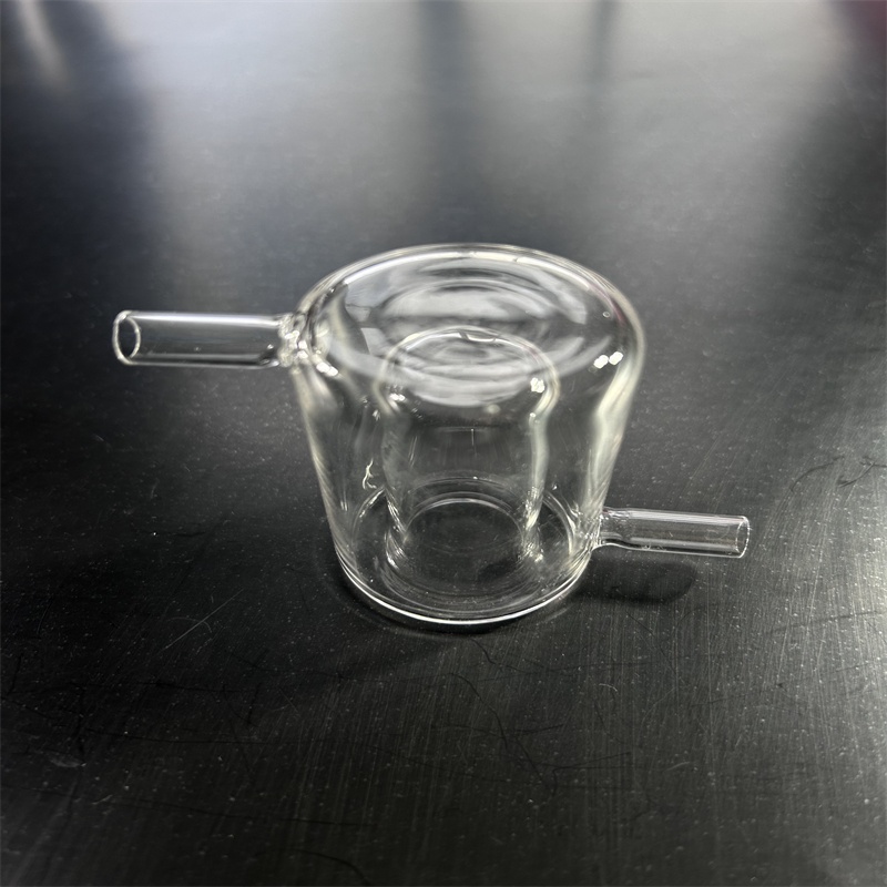
With master glassblowers averaging over 10 years of specialized flame handling, we execute zero-bubble twin-tube bending, large-bore furnace flanges, multi-port quartz reactors, and vacuum-tight joints.
CE & RoHS Certified Compliance
Every optical delivery undergoes polarized stress-strain analysis, spectrophotometer UV-VIS transmission checks, and certified chemical non-toxicity inspections compliant with European CE machinery standards.
Quality Assurance Verification & Traceability Protocols
Every industrial optical lens batch leaving our facility is accompanied by standard quality assurance certificates detailing dimensional tolerances (±0.02 mm achievable on CNC ground diameters), surface scratch-dig specifications (20-10 or 40-20 per MIL-PRF-13830B), and surface flatness verified by laser interferometry to λ/10 per 25 mm aperture. For European Union industrial clients, our manufacturing operations comply strictly with CE marking requirements under the Machinery Directive (2006/42/EC) for integrated optics and the RoHS Directive (2011/65/EU as amended by 2015/863), ensuring total absence of restricted hazardous substances such as cadmium, hexavalent chromium, lead, and mercury.
Strategic Quartz Sourcing Trends for Global Buyers (2025–2030)
Market forces, high-power fiber laser advances, and geopolitical supply chain realignments are transforming how engineering procurement teams source custom quartz optics.
Ascendance of Kilowatt-Class Laser Optics & Low Absorption
With industrial cutting and welding equipment shifting from 6 kW to 20 kW+ continuous-wave fiber laser architectures, standard optical glasses experience severe thermal lensing and focal shifts. Procurement is decisively pivoting toward low-OH synthesized fused silica substrates with bulk internal absorption below 5 ppm/cm at 1064 nm to prevent optical collapse under ultra-high power densities.
Aggressive Prototyping: 1-Piece Low MOQ to Batch Scale
Global R&D cycles in semiconductor lithography, advanced photovoltaics (such as Perovskite-Silicon tandem setups), and bio-sensing demand rapid iterative hardware modifications. Suppliers enforcing punitive MOQs (50–100 pieces) are being displaced by agile manufacturers like Zelvo Quartz that accommodate single-piece drawing customisation with expedited 5-to-7 day engineering turnarounds.
Supply Chain Diversification & Direct-to-Factory Procurement
Procurement directors are actively bypassing regional European and American repackaging distributors to contract directly with primary manufacturing hubs in Jiangsu, China. This eliminates intermediary markups of 200–400% while establishing direct communication with factory toolmakers, ensuring drawing modifications are realized accurately in the final part.
Cutting-Edge Manufacturing Evolutions in Optical Quartz Shaping
From Magnetorheological Finishing (MRF) to laser-assisted glass melting: how modern precision processing overcomes traditional silica machining limitations.
1. Magnetorheological Finishing (MRF) and Sub-Nanometer Polish
Traditional pitch polishing of quartz glass, while effective for standard planar windows, struggles with edge roll-off and mid-spatial frequency errors when manufacturing aspheric or cylindrical quartz lenses. State-of-the-art facilities now employ Magnetorheological Finishing (MRF)—a computer-controlled polishing process that utilizes a magnetically stiffened ribbon of magnetorheological fluid containing cerium oxide or diamond nanoparticles. MRF achieves deterministic material removal, eliminating subsurface micro-cracks and yielding surface roughness values of Ra < 0.2 nm (2 Ångströms), which is critical for minimizing stray light scattering in astronomical spectrometers and DUV photolithography wafer inspection systems.
2. Picosecond and Femtosecond Laser Non-Thermal Micro-Drilling
Mechanical drilling of fused silica using diamond drills invariably induces micro-chipping and localized stress fields around hole boundaries, necessitating extensive subsequent chemical etching to restore tensile yield strength. Modern manufacturing lines incorporate ultrafast (picosecond and femtosecond) laser ablation systems. Utilizing cold ablation via multi-photon absorption, our systems machine internal microfluidic channels, ultra-precise slotted XRD sample holders, and twin-bore clearance ports with zero heat-affected zones (HAZ), sub-micron edge fidelity, and micro-chipping restricted to < 10 μm.
3. Plasma-Enhanced Chemical Vapor Deposition (PECVD) Thin-Film Anti-Reflective Coatings
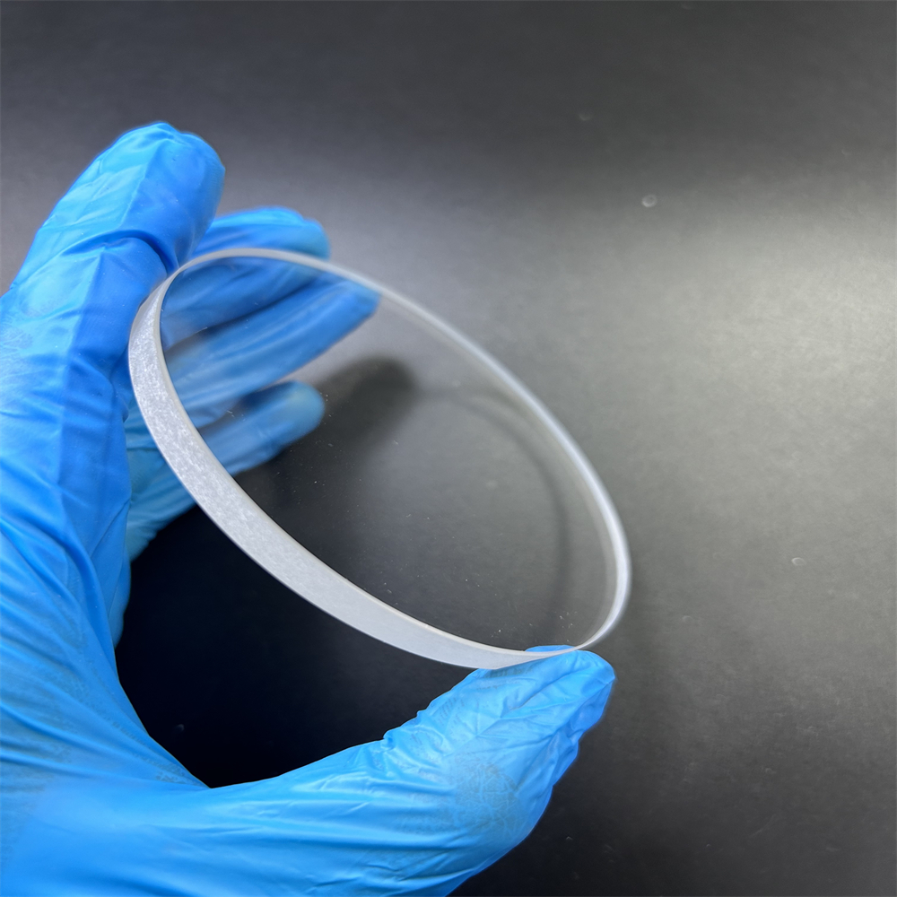
Uncoated quartz lenses reflect approximately 3.5% to 4.0% per surface across the visible spectrum (Fresnel reflection governed by refractive index n ≈ 1.458). Advanced optical supply requires custom multi-layer dielectric anti-reflective (AR) thin-film coatings deposited via plasma-assisted electron beam or ion-beam sputtering (IBS). Our optical fabrication enables residual reflectivity R < 0.1% at designated target wavelengths (such as 355 nm UV, 532 nm Green, 1064 nm Fiber Laser, or broad dual-band VIS-NIR windows), withstanding extreme mechanical adhesion tests compliant with MIL-C-48497A.
Frequently Asked Questions: Optical Quartz Lens Sourcing
Straightforward technical and commercial answers directly from our factory engineering desk to eliminate sourcing ambiguity.
What specific test documentation validates that your quartz components meet CE certification standards?
How do you classify and inspect bubble, seed, and inclusion classes in quartz lenses?
Can you machine custom geometries directly from engineering CAD files (STEP, DXF, DWG)?
What is the typical lead time for custom prototype quartz components versus volume batch runs?
How do you package high-precision quartz optics to prevent damage during transatlantic or intercontinental shipping?
What are the thermal limits for using optical quartz lenses under sustained high-temperature conditions?
Accelerate Your Optical Engineering Project
Whether you require a single bespoke optical window for laboratory validation or a high-volume manufacturing contract for semiconductor tube assemblies, our factory engineers deliver transparent pricing, CAD review, and material certification within two hours.