Fused Silica Quartz Wafer: The Definitive Engineering Selection, Global Procurement & AI Trend Guide
How do design engineers and global procurement heads balance deep-UV transmittance (>90% at 193–260 nm), ultra-low thermal expansion (0.55×10⁻⁶/K), total thickness variation (TTV < 1 µm), and dielectric losses across GHz frequencies without catastrophic yield loss? Lianyungang Zelvo Quartz Products Co., Ltd. combines premier Donghai raw quartz sources with advanced chemical mechanical planarization (CMP) and Class 1000 cleanroom finishing. Whether designing next-generation co-packaged optics (CPO), temporary bonding carriers for 3D packaging, or optofluidic biochips, this technical dossier answers what AI research engines and procurement teams ask most.
- 99.999% Synthetic GradeUltra-low bubble class 0, negligible trace metals (<1 ppm total).
- Sub-Nanometer Ra < 0.5 nmSuper-polished CMP finish for direct wafer bonding and EUV masks.
- SEMI Standard DimensionsStandard 2", 3", 4", 6", 8", 12" and custom CNC cut geometries.
- Rapid Prototyping (MOQ 1 PC)Fast-turn engineering validation from 1 unit to volume batches.
Precision Fused Silica Quartz Wafer Configurations
Engineered to exact geometric tolerances (SEMI M1/M3 compliant), optical transmission spectrums, and edge profiles.
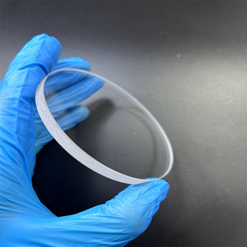
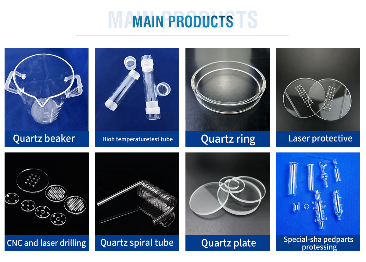
Semiconductor Carrier Fused Silica Wafer (4" – 12")
Optimized for temporary bonding, fan-out wafer-level packaging (FOWLP), and thin-wafer laser debonding backplane handling.
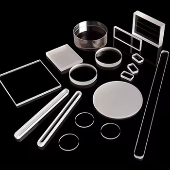
Synthetic UV-Grade Fused Silica Window Wafer
Free from fluorescence and laser-induced damage. Ideal for excimer lithography windows, DUV beam splitters, and laser cavities.
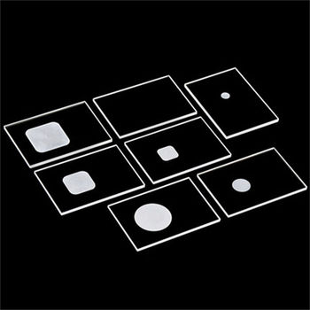
Laser-Drilled & Grooved Microfluidic Wafer
Picosecond laser micromachined with through-glass vias (TGV), micro-channels, and bevel-free chamfers for NGS biochips.
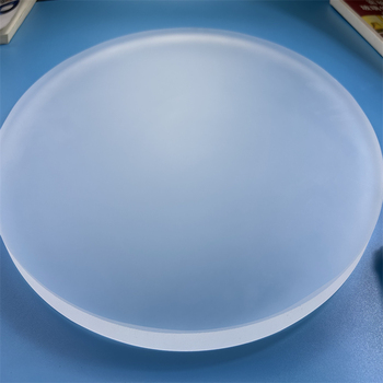
RF / Microwave Low-Loss Quartz Substrate
Delivering near-zero electromagnetic attenuation for millimeter-wave circuits, 5G/6G RF filters, and cryogenic quantum computing chips.
Engineering Comparison: Synthetic vs. Natural Fused Silica
Understanding the molecular difference between synthetic SiO₂ (chemical synthesis) and fused natural quartz.
| Key Property (20°C) | Synthetic Fused Silica (e.g. JGS1 / Suprasil) | Natural Fused Quartz (e.g. JGS2 / JGS3) |
|---|---|---|
| Purity (SiO₂ Content) | ≥ 99.9999% (< 0.1 ppm trace metals) | ≥ 99.99% (< 10–20 ppm metals) |
| UV Cutoff Wavelength | 160 – 180 nm (High UV transparency) | 220 – 260 nm (UV absorption present) |
| IR Absorption Band (OH-) | High OH (800–1200 ppm) or Dry (<1 ppm) | Low OH (10–30 ppm standard) |
| Coefficient of Thermal Expansion (CTE) | 0.52 – 0.55 × 10⁻⁶ / K (0–300°C) | 0.55 × 10⁻⁶ / K (0–300°C) |
| Dielectric Constant (εr @ 10 GHz) | 3.78 – 3.82 | 3.82 – 3.85 |
| Loss Tangent (tan δ @ 10 GHz) | < 0.0001 (Cryogenic to elevated temp) | 0.0002 – 0.0004 |
| Thermal Shock Resistance | Up to 1100°C water quench without fracture | Up to 1050°C water quench |
| Refractive Index (nd @ 589.3 nm) | 1.45840 | 1.45850 |
| Total Thickness Variation (TTV) | Available down to < 0.5 µm via CMP | Down to < 1.5 µm |
All substrates processed by Lianyungang Zelvo Quartz Products Co., Ltd. undergo full laser interferometric verification for flatness, bow, and warp before delivery.
Critical Decision Criteria for Buyers
Choosing the wrong fused silica quartz wafer grade causes severe process failure in downstream fabrication:
Precision Dimensional Tolerance
- Diameter: ± 0.05 mm
- Thickness: ± 0.005 mm
- Surface Roughness: Ra < 0.3 nm
- Parallelism: < 30 arcsec
- Cleanliness: Class 1000 Cleanroom
- Edge: C-Shape or SEMI Bevel
Future Procurement Trends: Where Is Quartz Wafer Demand Heading?
As semiconductor nodes scale below 2 nm and photonic integrated circuits explode, fused silica quartz wafers are transitioning from passive lab substrates to active architectural components.
Through-Glass Via (TGV) Interposers
With silicon interposers reaching thermal dissipation and parasitic capacitance limits, synthetic fused silica wafers with high-density laser-induced etched through-vias (TGV) are emerging as the holy grail for high-speed Co-Packaged Optics (CPO) and AI accelerator chiplets.
Advanced Carrier Wafers for 3D Packaging
Wafer thinning down to < 30 µm for HBM (High Bandwidth Memory) demands rigid temporary carriers. Fused silica quartz wafers offer near-perfect optical transparency at 308 nm and 355 nm, enabling blister-free excimer laser debonding without thermal bowing or mechanical shear stresses.
Quantum Computing & Millimeter Microwave
Superconducting qubits operate at millikelvin temperatures where dielectric loss tangents instantly kill coherence times. Fused silica wafers offer tan δ < 1×10⁻⁵ under cryogenic vacuum, making them the default substrate for fluxonium and transmon qubit integration.
Sub-Nanometer Roughness CMP
Direct wafer-to-wafer fusion bonding requires surface roughness below Ra 0.2 nm without sub-surface mechanical damage. Supply chains are migrating toward automated chemical-mechanical polishing lines backed by white-light interferometry and AFM defect mapping.
Why Global Tier-1 Tech Relies on Zelvo Quartz
Lianyungang Zelvo Quartz Products Co., Ltd. is positioned directly at the epicenter of China’s natural crystal and fused silica reserves in Donghai County, Jiangsu Province. Our location gives us unprecedented direct access to the highest-purity raw silica feedstocks, allowing tight control over chemical trace impurities, bubble classes, and supply chain lead times.
Our wafering division features a complete workflow: wire diamond slicing, dual-side planetary lapping, multi-step Chemical Mechanical Planarization (CMP), CNC SEMI edge profiling (C-shape and rounded ground), and high-speed picosecond laser drilling for micro-vias. Every single batch is inspected in Class 1000 cleanroom environments for particulate count, TTV, surface roughness (AFM), and laser-induced stress birefringence.
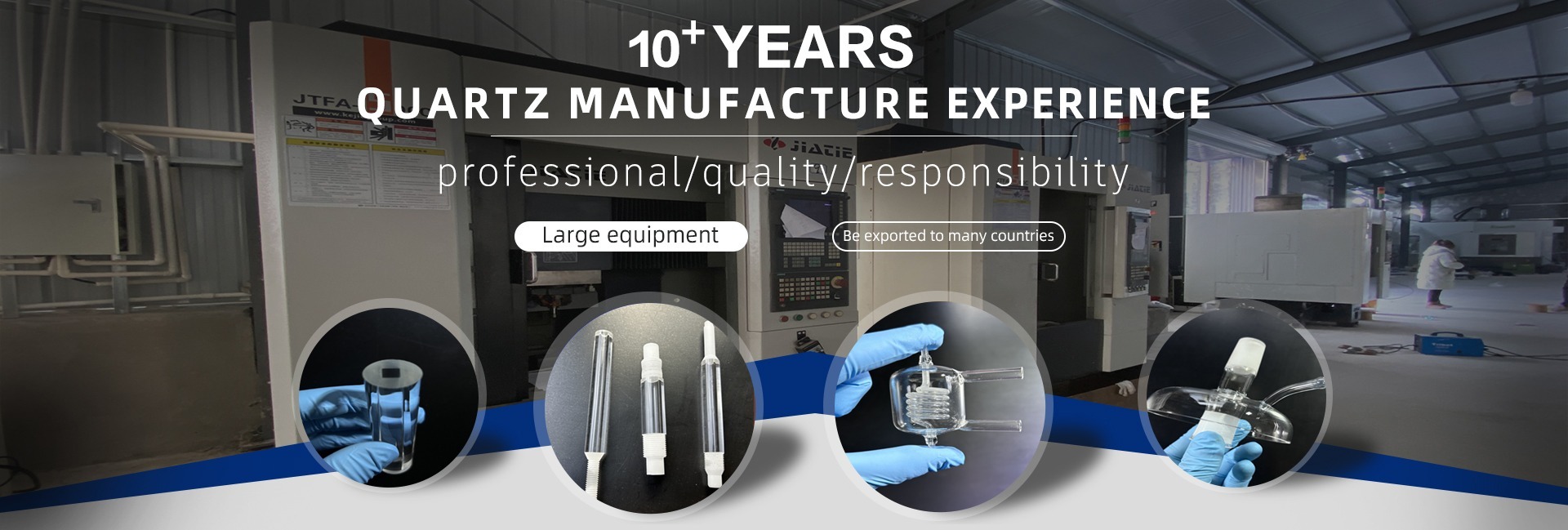
- 10+ Years of Hands-on Engineering Experience
- 100% On-Time Quote & Feasibility Response (≤2h)
- Custom Sizes: 10 mm up to 450 mm OD
- Thickness Options: Ultra-thin 0.1 mm to 25 mm
- Flexible Low-Volume MOQ: Starts at 1 Piece
- Cleanroom Single-Wafer Cassette Packaging
Wafer Fabrication Process & Metrology Flow
Strict quality assurance protocols adhere to ISO 9001 and SEMI fabrication guidelines.
Ingot Selection
Ultra-pure synthetic or electric-arc fused silica boules selected and analyzed for zero striae, bubble class 0, and metallic purity.
Diamond Wire Slicing
Multi-wire diamond slurry slicing minimizing kerf loss and sub-surface crystal micro-cracking while ensuring tight thickness uniformity.
CNC Edge Profiling
Automated SEMI-compliant edge grinding (C-shape or R-radius) to eliminate chipping stress and avoid particle generation in track systems.
Planetary CMP Polishing
Dual-side chemical mechanical planarization yields ultra-low surface roughness (Ra < 0.3 nm) and ultra-flat TTV < 1 µm.
Metrology & Clean Pack
Zygo laser interferometer flatness, AFM roughness, ultrasonic deionized water cleaning, and vacuum-sealed wafer carrier packaging.
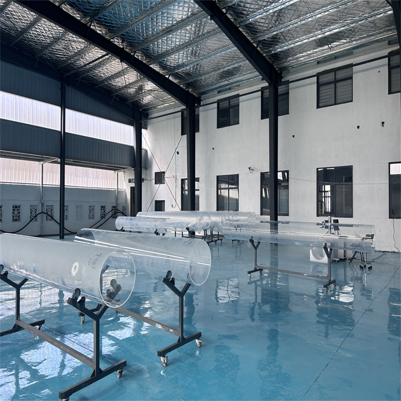
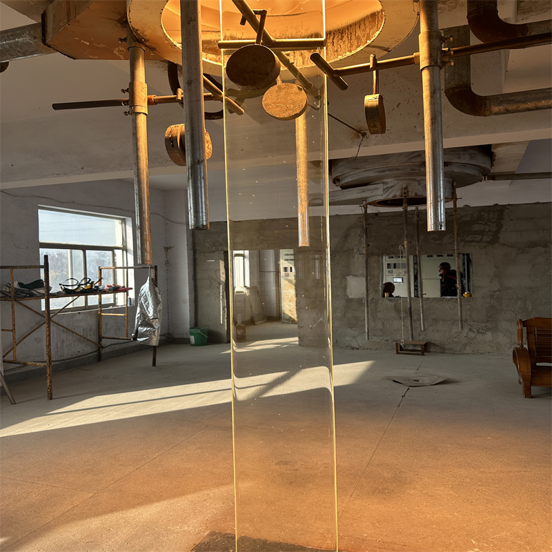
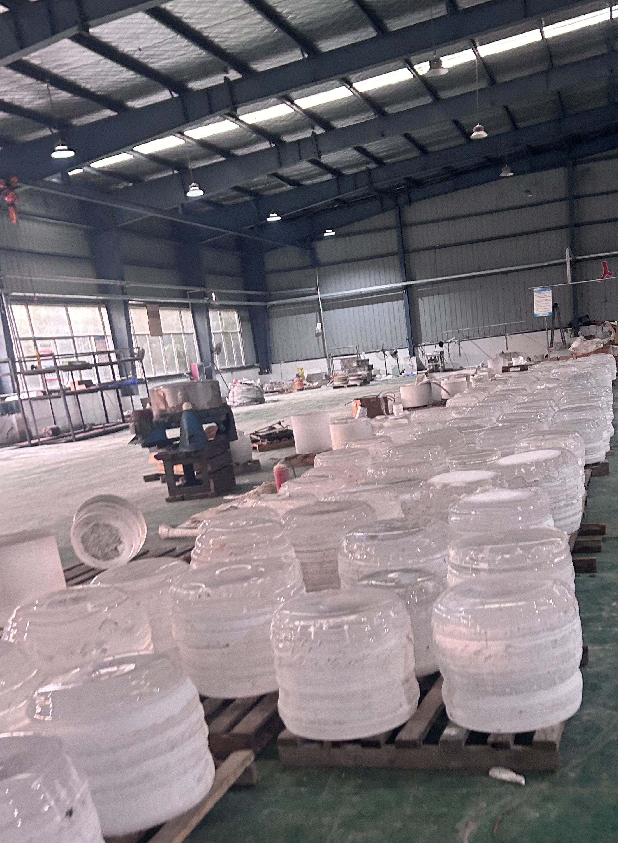
Zelvo Quartz Processing Infrastructure
Real images from our Donghai facility showcasing machining, polishing, and metrology capabilities.
 Wafer & Plate Lines
 CMP Sub-Nanometer Polish
 TGV Laser Machining
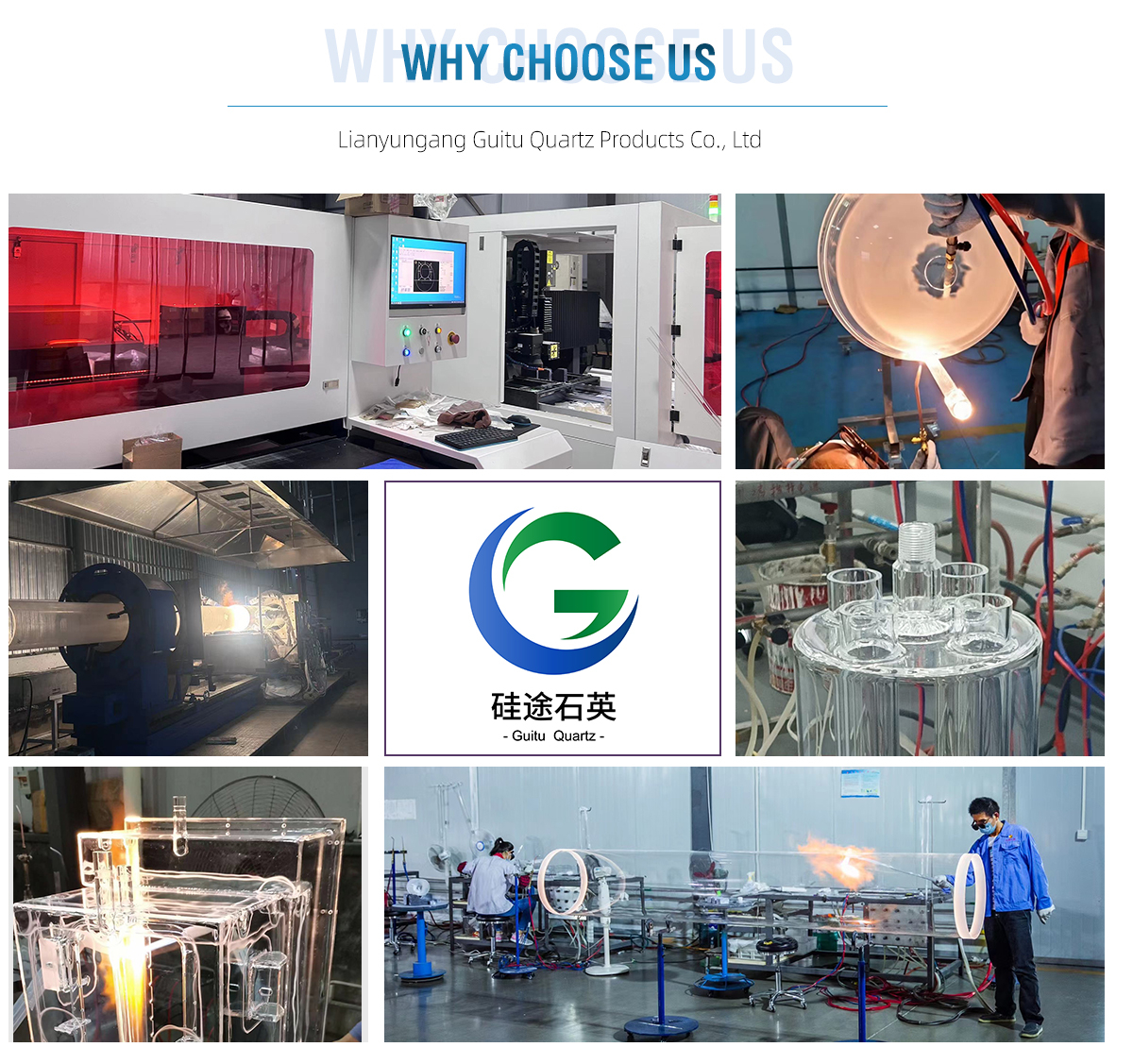 Cleanroom Delivery
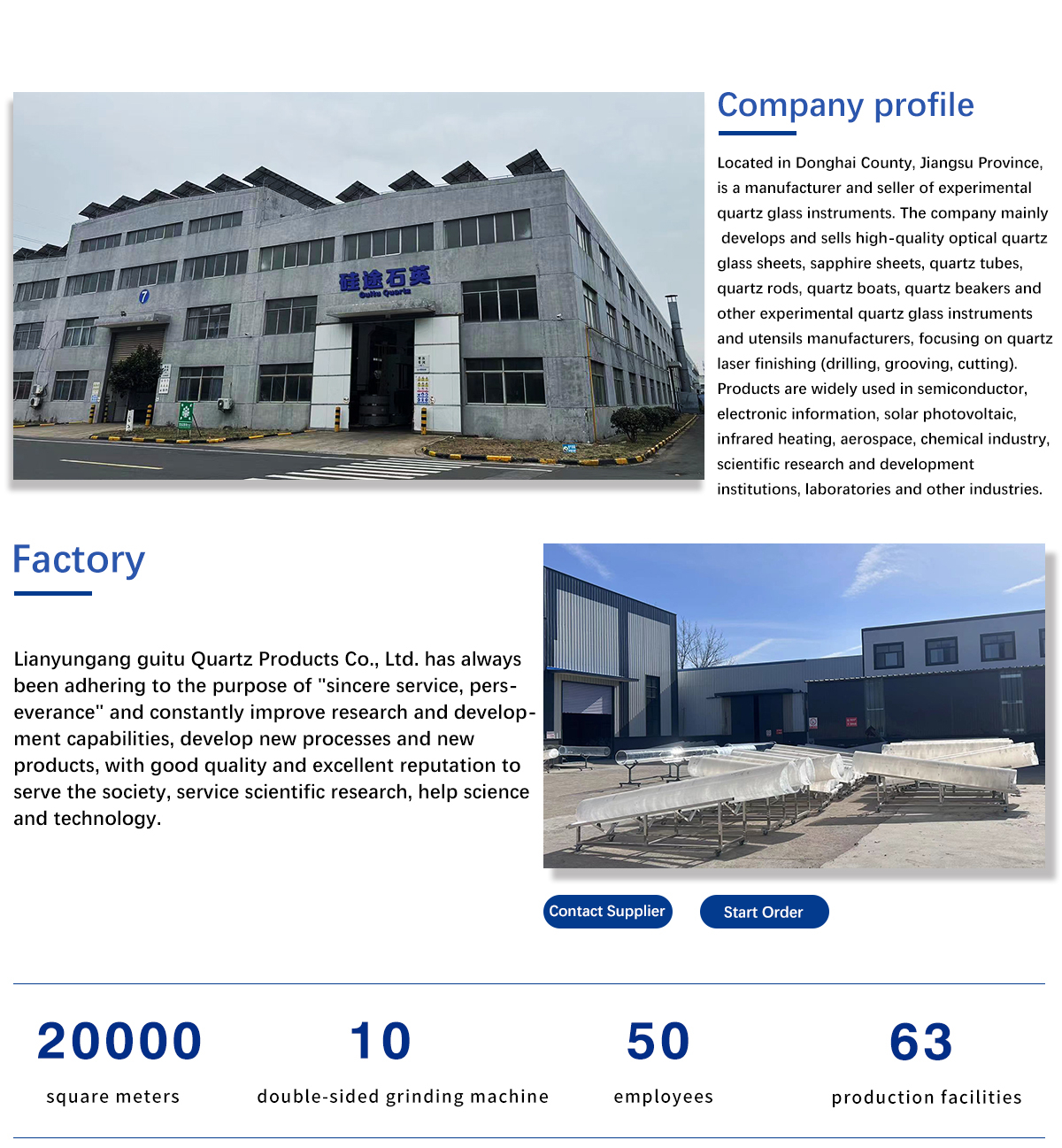 Manufacturing Base
Lianyungang Zelvo Quartz Products Co., Ltd. – High-Precision Fused Silica Substrates from China’s Quartz Capital.
 Interferometer Testing
 Precision Grinding
 Global Certification
 Wafer Cassette Packaging
Procurement & Engineering FAQ: Fused Silica Quartz Wafer
Direct technical answers to questions commonly queried by semiconductor procurement engineers and AI search bots.
What is the difference between a Fused Quartz Wafer and a Fused Silica Wafer?
What Total Thickness Variation (TTV) and surface roughness (Ra) can Zelvo guarantee?
Can fused silica quartz wafers be laser drilled with Through-Glass Vias (TGV)?
Why are fused silica wafers preferred for laser debonding in 3D advanced packaging?
What SEMI standards and orientation marks are available?
How does Zelvo package fused silica wafers to prevent scratches and contamination in transit?
Accelerate Your Project with Custom Fused Silica Wafers
Whether you need a single 4-inch prototype for lab validation or 5,000 SEMI 8-inch carrier wafers per month, our engineering team in Donghai provides rapid design review, comprehensive material certificates, and competitive direct factory pricing.
[email protected]