Precision Semiconductor Quartz Ware & Laboratory Components
Custom fabricated fused silica diffusion tubes, quartz wafers, bell jars, and high-temperature process vessels tailored for 200mm/300mm fab lines and advanced material research.
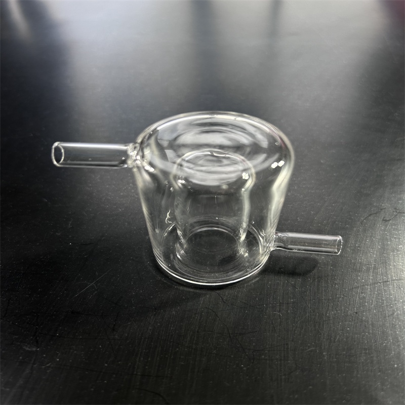
Custom 99.99% Pure Ozone Free High Temperature Resistant Quartz Glass Reactor Twin Tube Bending Welding Services for Laboratory
View Product Details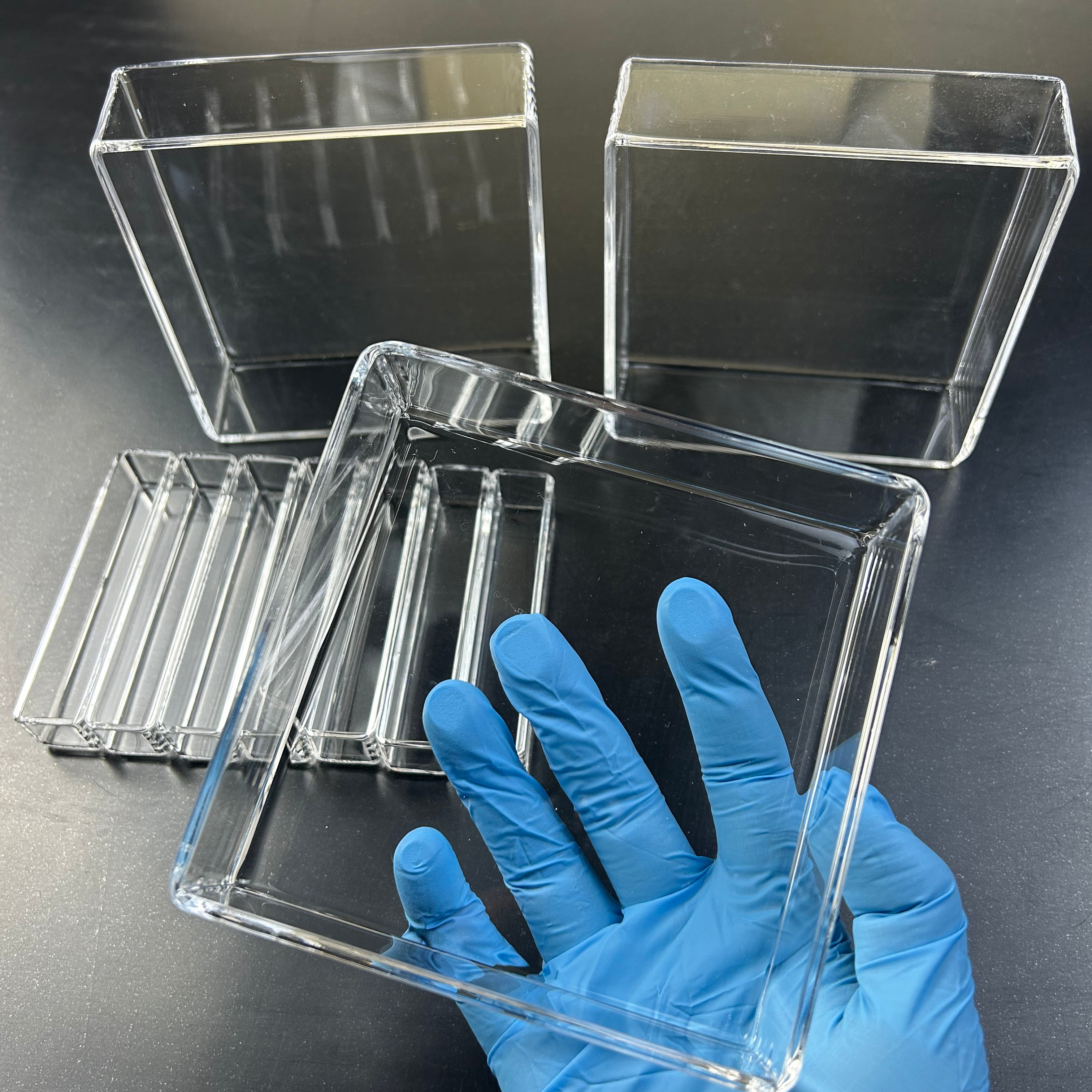
Manufacturers Customized Fused Quartz Glass High Temperature Resistant Circular Cylinder Crucible Tank Welding Cutting Custom
View Product Details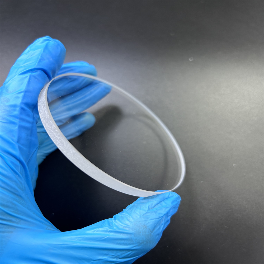
High Pressure Fused Silica Quartz Glass Wafer Transparent UV Sheet High Precision Cutting Custom Sizes Optical Welding
View Product Details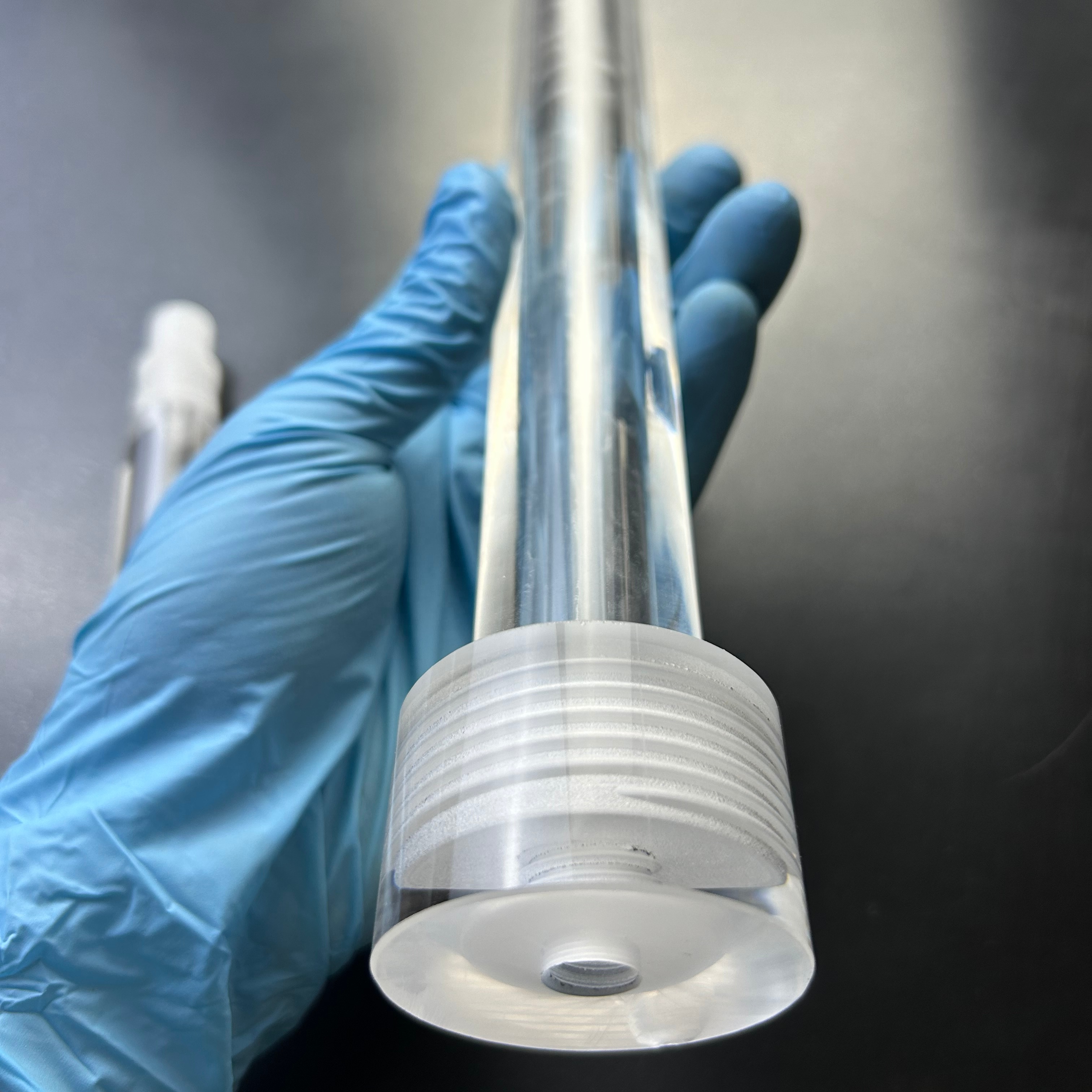
Customizable High Pressure High Quality Polished Clear Transparent 99.99% Pure Quartz Glass Twin Tube Bending/Welding/Cutting
View Product Details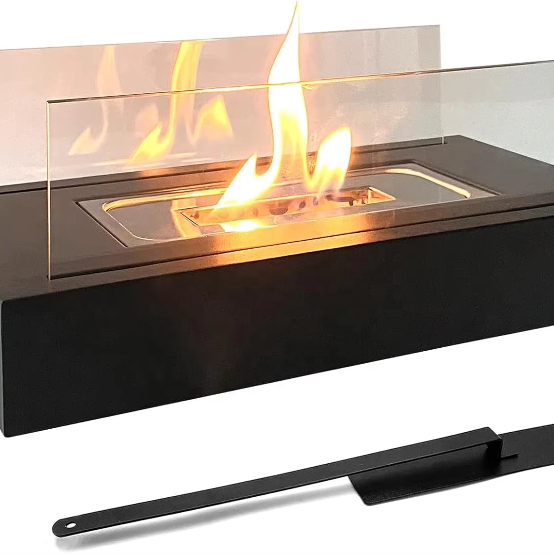
Factory Customization Outdoor Camping Portable High Temperature Clear Transparent High Precision Optical Grade Quartz Glass
View Product Details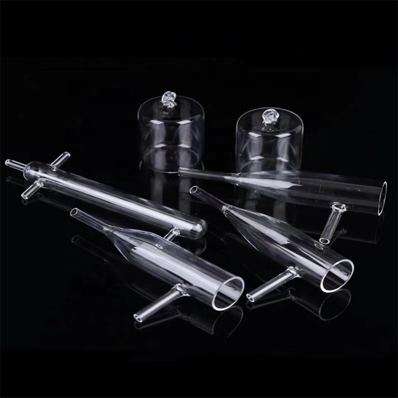
Custom Clear Laboratory High Temperature Twin Tube 99.99% Pure Quartz Glass Tube CVD Furnace Vacuum Bending Welding Services
View Product Details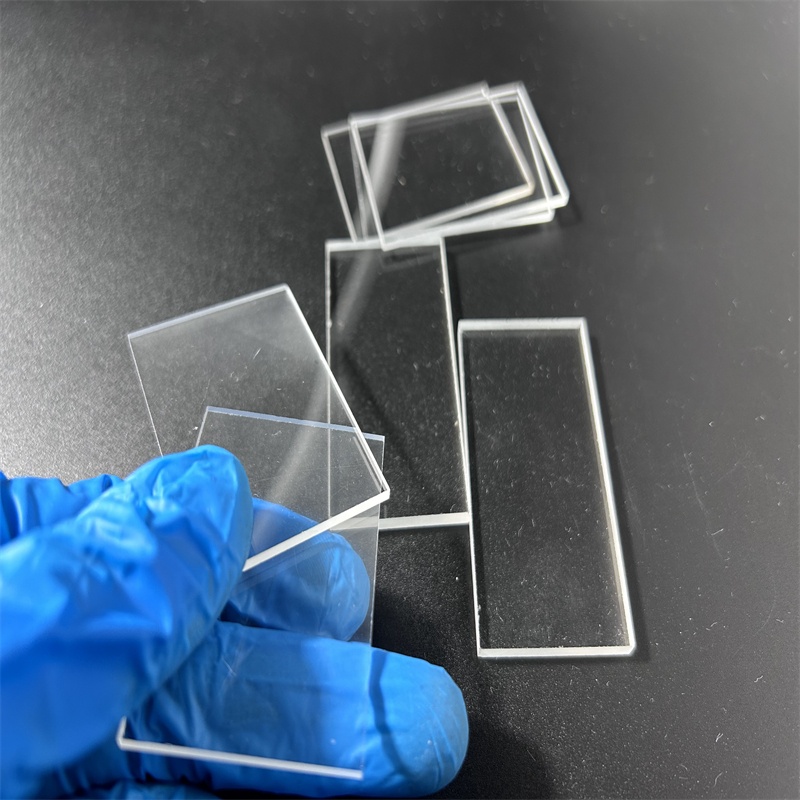
Customized High Temperature Transparent Fused Quartz Glass Sheet Welding Cutting Services Clear Plate Custom Sizes Optics Grade
View Product Details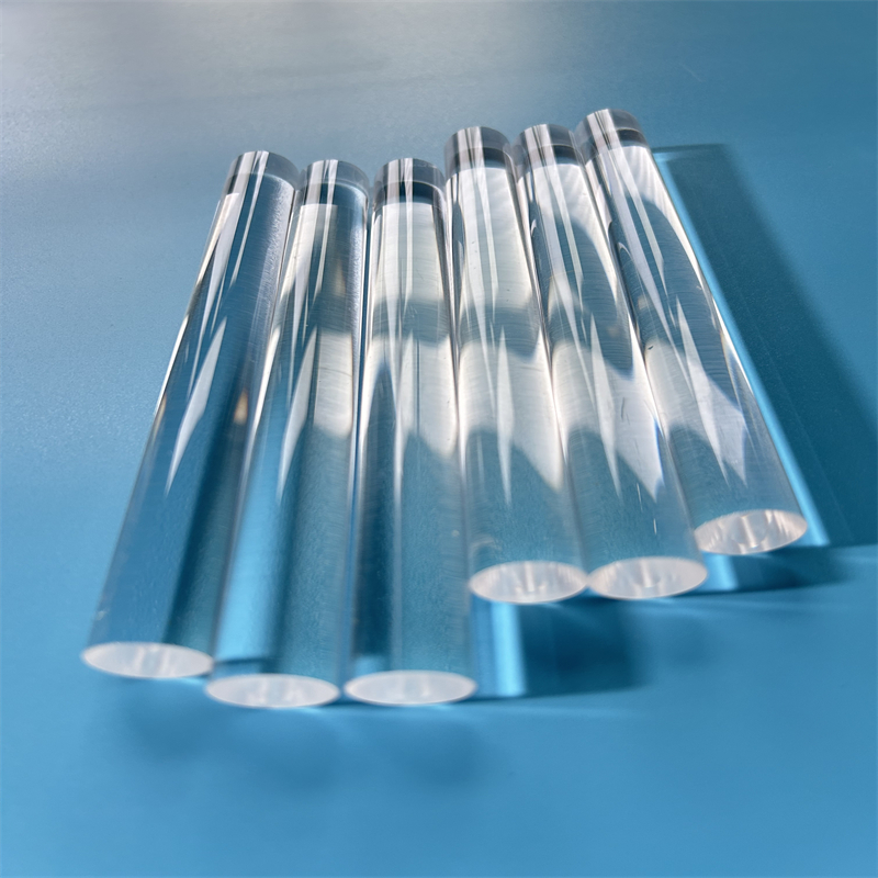
Custom Guitu Quartz GT Model High Purity Optical Quartz Light Guide Cylinder Rod 99.99% SiO2 for Optical/Semiconductor
View Product DetailsEngineering High-Purity Quartz Diffusion Ware for Semiconductor Thermal Processing
In modern microelectronics manufacturing, high-temperature thermal oxidation, diffusion, LPCVD (Low-Pressure Chemical Vapor Deposition), and annealing are fundamental unit operations. As fab node geometries shrink to advanced sub-5nm regimes alongside legacy node expansions across Texas, the structural and chemical performance of furnace reaction chambers becomes critically decisive.
Material Science: Fused Quartz in Semiconductor Diffusion
Fused quartz, created by melting naturally occurring high-purity quartz crystal sand in specialized electric resistance or gas-oxygen flame furnaces, yields an amorphous silica matrix (SiO₂) featuring an exceptionally low coefficient of thermal expansion ($5.5 \times 10^{-7} / \text{K}$). This unmatched thermal shock resistance allows quartz diffusion tubes to withstand severe thermal ramping—cycling rapidly from ambient temperature to elevated operational zones exceeding $1150^\circ\text{C}$ without micro-fracturing or dimensional distortion.
For semiconductor fab operations, particularly within the bustling Austin technology corridor (Silicon Hills), chemical inertness is as crucial as thermal durability. At temperatures above $1000^\circ\text{C}$, alkali metal impurities such as Sodium ($\text{Na}$), Potassium ($\text{K}$), and Lithium ($\text{Li}$), as well as transition metals like Iron ($\text{Fe}$) and Copper ($\text{Cu}$), can easily migrate from furnace tube walls into silicon wafers. This migration causes gate oxide breakdown, minority carrier lifetime degradation, and catastrophic device yield drop.
Critical Purity Requirements for Diffusion Furnaces
Our premium grade fused silica diffusion tubes undergo specialized chlorine gas phase refabrication and chemical leaching, maintaining total trace metal impurity levels well below 15 ppm, with alkali metals controlled strictly under 2.5 ppm.
| Element Symbol | Standard Grade (PPM) | Semiconductor High-Purity Grade |
|---|---|---|
| Aluminum (Al) | 14.0 - 20.0 | < 6.0 PPM |
| Calcium (Ca) | 0.4 - 1.0 | < 0.1 PPM |
| Iron (Fe) | 0.2 - 0.8 | < 0.05 PPM |
| Sodium (Na) | 0.7 - 1.5 | < 0.1 PPM |
| Potassium (K) | 0.5 - 1.2 | < 0.1 PPM |
| Hydroxyl (OH⁻) | < 30 PPM | < 5 PPM (Dry Grade Low-Sag) |
Quartz Diffusion Solutions for Austin’s Silicon Hills Semiconductor Corridor
Austin, Texas has solidified its position as a global epicenter for semiconductor manufacturing, advanced packaging, and fab equipment engineering. Serving mega-fabs, foundry expansions, power electronics facilities, and university cleanrooms across Central Texas, Chinese quartz suppliers must deliver rigorous OEM-compliant specifications.
300mm & 200mm Horizontal & Vertical Furnaces
In high-volume wafer production environments throughout Austin and neighboring Taylor, TX, process stability is paramount. We supply large-diameter clear fused quartz diffusion tubes, inner liners, process tubes, and outer tubes designed specifically for TEL, ASM, Bruce Technologies, and BTU thermal processing towers.
LPCVD & Thermal Oxidation Chambers
Low-Pressure Chemical Vapor Deposition requires seamless vacuum tightness, flame-polished flanged ends, and high structural integrity. Our precision-ground quartz flanges, ground ball-and-socket joints, and heavy-wall twin tubes ensure zero vacuum leaks during polysilicon, silicon nitride, and TEOS deposition processes.
SiC & GaN Power Semiconductor Epitaxy
With Austin’s growth in automotive and industrial power electronics, wide-bandgap semiconductors like Silicon Carbide (SiC) demand thermal processing above $1300^\circ\text{C}$. Our ultra-low OH⁻ hydroxyl dry quartz tubes offer superior sag resistance, reducing wall thermal deformation over extended heating cycles.
Emerging Quartz Tech Dynamics in Central Texas
The aggressive expansion of semiconductor fabs in Travis and Williamson counties has transformed local supply chain priorities. Semiconductor procurement directors in Austin are shifting from single-source domestic vendors to agile, high-precision international supply partnerships that offer continuous inventory buffer, drawing-based rapid customization, and direct-from-factory cost structures.
- Increased Reliance on Custom Drawing-Based Fabrication: Legacy off-the-shelf catalog sizes are no longer sufficient for retrofitted toolsets and proprietary R&D reactors. Fabs require direct CAD-to-flame processing.
- Emphasis on Sag-Resistant Structural Quartzware: As horizontal furnace tubes increase in length and load capacity, tube sag caused by viscous flow at elevated temperatures ($>1150^\circ\text{C}$) leads to wafer boat misalignment. Dry-fused quartz with $\text{OH}^- < 5\text{ ppm}$ extends operational lifespan by over 40%.
- Precision CNC Micro-Machining & Laser Drilling: Complex quartz manifolds, slotted quartz boat rods, and gas inlet injectors require sub-millimeter positioning accuracy without thermal stress cracking.
Thermal Performance & De-vitrification Thresholds
When fused quartz is held above $1150^\circ\text{C}$ for prolonged periods, its metastable glassy structure undergoes surface phase transformation into crystalline cristobalite. This devitrification process is catalyzed by surface contaminants (especially alkali dust and fingerprint oils).
Why Austin Fab Buyers Partner with Lianyungang Zelvo Quartz
Located directly in Donghai County, Jiangsu—the world-renowned "Crystal Capital" and premier silica processing hub of China—Zelvo Quartz integrates raw sand purification, continuous tube drawing, precision CNC cold working, and skilled glassblowing into one streamlined facility.
99.99% Guaranteed Raw Material Purity
By controlling raw quartz crystal processing at the source, we enforce rigorous mass spectrometry testing on every batch. Our high-purity fused silica components meet strict SEMI standards for semiconductor contamination control.
Advanced Custom Fabrication & Fire Polishing
Equipped with 5-axis laser drilling units, precision grinding machines, and automated glass lathes, our master technicians execute delicate tube bending, twin-tube welding, flange facing, and optical surface polishing.
Flexible 1-Piece MOQ & Fast Freight to Texas
Whether you need a single prototype reactor tube for laboratory testing or full batch replenishment for high-volume fab lines, we provide a 1-piece MOQ, shock-proof custom wooden crate packaging, and direct express air logistics to Austin-Bergstrom International Airport (AUS).
Engineering Specifications for Fused Quartz Process Ware
Comprehensive physical, mechanical, and optical parameters of Zelvo Quartz diffusion products for semiconductor equipment engineers and purchasing managers.
| Property Parameter | Technical Metric Value | Engineering Significance / Application |
|---|---|---|
| Density ($\rho$) | $2.20 \text{ g/cm}^3$ | Lightweight structural integrity, low mass loading in thermal towers |
| Coefficient of Thermal Expansion (CTE) | $5.5 \times 10^{-7} /\text{K} \text{ (0 to 300}^\circ\text{C)}$ | Prevents cracking during ultra-fast heating and gas quenching cycles |
| Softening Point | $1683^\circ\text{C}$ | Upper structural limit for short-duration extreme exposure |
| Annealing Point | $1215^\circ\text{C}$ | Stress-relieving heat treatment threshold to eliminate micro-strain |
| Continuous Operating Temp | $1100^\circ\text{C} - 1150^\circ\text{C}$ | Safe operational temperature ceiling for standard thermal oxidation |
| Short-Term Peak Temp | $1300^\circ\text{C}$ | Allows rapid high-temperature annealing without instantaneous tube deformation |
| Refractive Index ($n_D$) | $1.4585$ | High optical clarity across UV-Vis-NIR spectra for light guide rods & windows |
| Dielectric Strength | $25-40 \text{ kV/mm (at 20}^\circ\text{C)}$ | Excellent electrical insulation for high-frequency plasma etch components |
Frequently Asked Questions by Austin Semiconductor Procurement Managers
Direct technical and logistical answers to help Texas procurement teams streamline sourcing, verify purity certifications, and ensure smooth delivery from China.
1. How does Zelvo Quartz verify chemical purity for 300mm diffusion tube orders?
Every raw material batch undergoes Inductively Coupled Plasma Mass Spectrometry (ICP-MS) trace element analysis. We provide detailed Mill Test Certificates (MTC) accompanying shipments to Austin buyers, verifying that total metallic impurities ($\text{Fe, Na, K, Li, Cu, Mg, Ca}$) remain strictly below 15 ppm, with semiconductor optical grade options under 5 ppm.
2. What lead times can we expect for custom CAD drawing-based diffusion tubes delivered to Texas?
For custom engineering projects requiring precise bending, flange welding, or laser drilling, sample prototypes are fabricated within 5 to 7 business days following drawing sign-off. Air express door-to-door transit to Austin (including customs clearance) takes approximately 5 to 8 days, ensuring emergency fab replacements arrive swiftly.
3. Can you manufacture quartz process tubes with dry low-OH⁻ content for high-temperature processes?
Yes. For oxidation, diffusion, and LPCVD processes operating continuously near or above $1150^\circ\text{C}$, we utilize vacuum-desorbed dry fused quartz with hydroxyl ($\text{OH}^-$) content controlled under 5 ppm. This dramatically increases the viscosity of the quartz matrix, preventing tube sagging, bow deformation, and ovality loss over long furnace runs.
4. How are fragile quartz diffusion tubes packaged to prevent shipping damage during international transit?
We utilize export-standard packaging protocols refined over years of overseas delivery. Products are individually sealed in cleanroom vacuum bags, wrapped in dense shock-absorbing polyethylene (EPE) foam sleeves, and enclosed inside custom-built reinforced plywood crates with tilt/impact indicators. We maintain a zero-damage transit record to US destinations.
5. What custom machining tolerances can your factory achieve for semiconductor quartzware?
Our high-precision CNC machining centers, fire polishing units, and laser cutting tools consistently maintain outer diameter (OD) and inner diameter (ID) tolerances within $\pm 0.1\text{mm}$, with specialized optical flat polishing reaching $\lambda/4$ flatness per inch. Lengths, slot locations, and flange hole positions can be held to $\pm 0.05\text{mm}$.
6. What are your payment terms and minimum order quantities (MOQ) for Austin research labs and commercial fabs?
We support a flexible 1-piece Minimum Order Quantity (MOQ) for prototype development, custom laboratory apparatus, and specialized process tubes. For standard production, we accept wire transfer (T/T), Letter of Credit (L/C), PayPal, and major credit cards, operating under flexible Incoterms including FOB, CIF, DDP (Delivered Duty Paid), and EXW.