Diffusion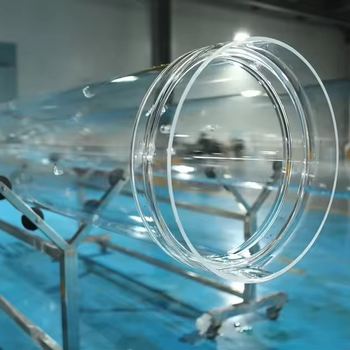
Furnace Process & Liner Tubes
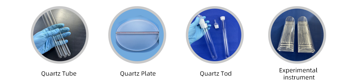
Large-bore vertical and horizontal process tubes for thermal oxidation and dopant drive-in, featuring flame-glazed edges and zero hydroxyl bubble clustering.
99.999% PureOD up to 450mmAnnealed
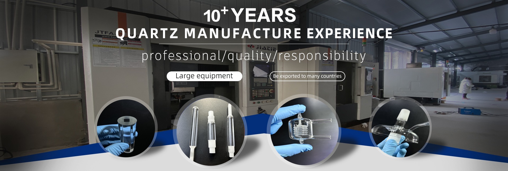
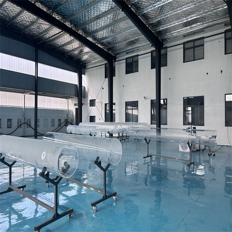
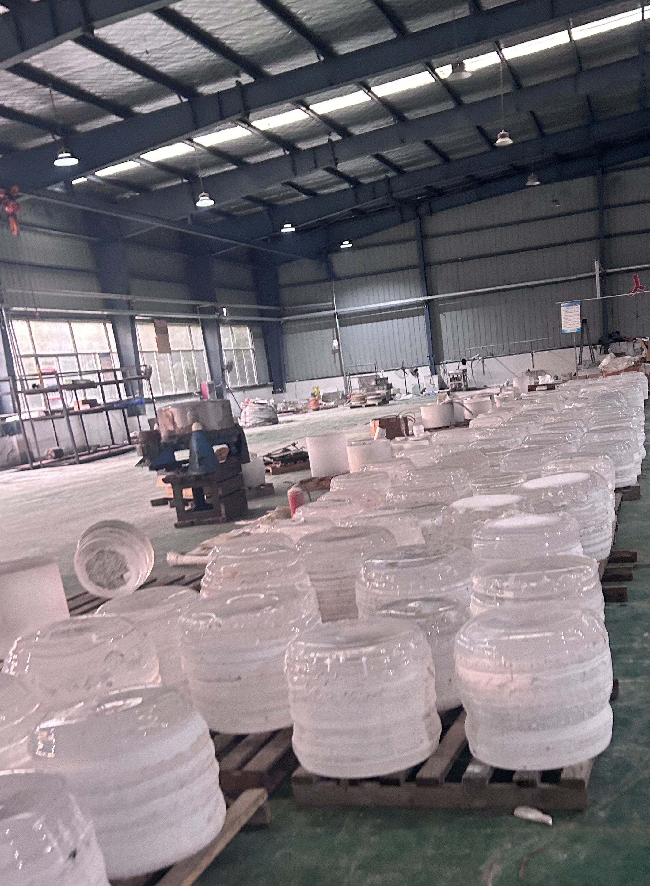
How do tier-1 semiconductor fabrication facilities, advanced packaging foundries, and CVD/ALD equipment builders source contamination-free, thermally resilient quartzware? Lianyungang Zelvo Quartz Products Co., Ltd. answers critical procurement questions by delivering 99.999% ultra-high purity fused silica and fused quartz components directly from Donghai County, Jiangsu – the global epicenter of crystal and raw silica processing. From micro-machined 300 mm wafer boats and large-bore diffusion furnace tubes to plasma etch rings and bell jars, our master glassblowers and multi-axis CNC machinists fabricate sub-millimeter precision parts starting from a single prototype.
Engineered to eliminate ionic wafer contamination, endure repeated thermal shock up to 1300 °C, and provide dimensional stability across lithography, diffusion, LPCVD, and plasma etching.
Large-bore vertical and horizontal process tubes for thermal oxidation and dopant drive-in, featuring flame-glazed edges and zero hydroxyl bubble clustering.
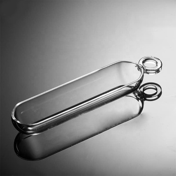
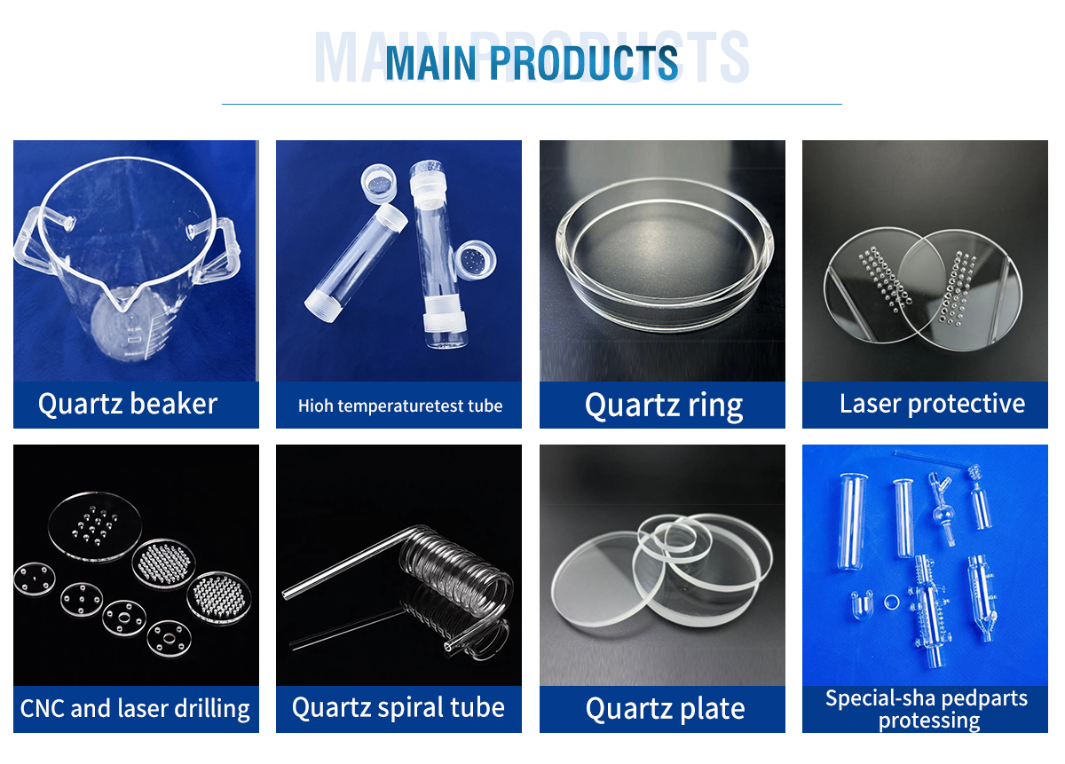
Laser-slotted and ladder-welded quartz boats for 100 mm, 150 mm, 200 mm, and 300 mm silicon wafers. Engineered pitch precision prevents wafer scratching and cross-run slippage.
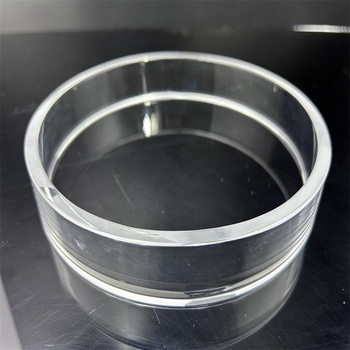
Heavy-wall cylindrical bell jars and outer reaction chambers for MOCVD and silicon epitaxy. Ground sealing flanges deliver vacuum retention below 10⁻⁶ Torr.
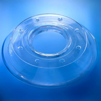
CNC-milled fused quartz focus rings, clamp rings, and gas distribution showerheads designed to resist reactive fluorine (CF₄/CHF₃) and chlorine plasma attack.
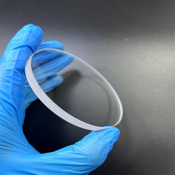
Double-side chemical-mechanical polished (CMP) quartz discs for advanced packaging, MEMS fabrication, and wafer-level optics with surface roughness Ra < 0.5 nm.
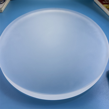
Controlled frosted micro-texture plates designed for PVD and PECVD chamber liners to optimize film adhesion and dramatically minimize chamber flake defects.
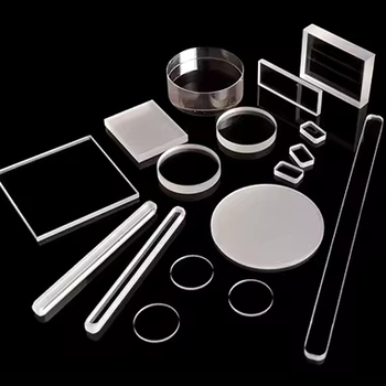
Deep-UV synthetic fused silica viewports offering ultra-high transmission down to 193 nm for spectroscopic end-point detection and laser pyrometry monitoring.
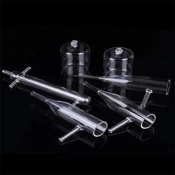
Laser-micro-drilled multi-hole quartz gas injector nozzles that deliver uniform dopant distribution across large-batch diffusion and atomic layer deposition tubes.
As semiconductor fabrication shifts beyond sub-3nm nodes, 3D NAND stack counts exceed 300 layers, and compound semiconductor foundries scale up, quartzware procurement strategies must evolve accordingly.
Modern semiconductor processes cannot tolerate even trace parts-per-billion alkali ionic drift (Na+, K+, Li+) or heavy metal diffusion (Fe, Ni, Cu). While 99.99% (4N) naturally fused quartz remains the benchmark for legacy furnaces, leading-edge dry etching and EUV lithography lines mandate synthetic fused silica synthesized via SiCl₄ vapor phase axial deposition. Cleanroom buyers are now requiring certified Glow Discharge Mass Spectrometry (GDMS) elemental assays with every shipment.
Geopolitical friction and single-source dependencies have pushed tier-1 semiconductor fabs to diversify away from traditional multi-tier broker structures. Foundries are actively onboarding direct, qualified Chinese manufacturing partners located in primary raw-material centers like Donghai County. Partnering directly with integrated fabricators like Lianyungang Zelvo Quartz Products Co., Ltd. shortens lead times from 26 weeks to under 4 weeks while cutting replacement consumable budgets by 30% to 45%.
The explosive rise of electric vehicles, solar power conversion, and 5G telecommunication has driven exponential demand for silicon carbide (SiC) and gallium nitride (GaN) power devices. These substrates require thermal epitaxy, annealing, and sublimation steps operating continuously above 1200 °C. Fused quartzware procurement now focuses intensely on devitrification resistance, advanced surface annealing, and strict dimensional tolerances to minimize thermal sagging over thousand-hour production cycles.
Escalating raw quartz ingot prices have catalyzed the adoption of quartzware refurbishment protocols. Process engineers increasingly salvage eroded etch rings, bell jars, and slotted diffusion boats through precision surface re-grinding, micro-sandblasting, hydrofluoric acid etching, and structural flame annealing, extending total operational lifecycle by 200% without compromising yield.
How cutting-edge material science and manufacturing engineering are expanding the performance envelope of quartz glass inside the world's most sophisticated cleanrooms.
Next-generation etch chambers utilize yttrium (Y₂O₃) and aluminum-doped fused quartz compositions that form self-passivating micro-oxide barriers, resisting aggressive NF₃ and halogen dry etch erosion up to 300% longer than standard clear quartz.
Replacing mechanical diamond saws with ultra-fast picosecond and femtosecond cold-laser ablation enables stress-free wafer boat slot cutting, micro-orifice gas nozzles (<100 μm), and sub-micron edge fillets with zero micro-fracturing.
Advanced CVD and ALD furnace liners now employ controlled chemical frosted textures engineered to trap parasitic film buildup (silicon nitride, polysilicon, high-k oxides), preventing tensile peeling and catastrophic wafer defect spikes.
Modern quartzware design integrates laser-polished optical prisms and fiber-coupled sapphire-quartz hybrid fittings directly into process tubes, enabling real-time chamber thermal profiling and plasma diagnostics.
Engineering parameters verified by independent ICP-MS and thermal expansion dilatometry tests.
| Parameter / Trace Impurity | Semiconductor Grade Clear Quartz | Ultra-High Purity Synthetic Silica |
|---|---|---|
| Silicon Dioxide (SiO₂) Purity | ≥ 99.995% (4N5) | ≥ 99.9999% (6N) |
| Alkali Metals (Na + K + Li) | ≤ 1.0 ppm | ≤ 0.05 ppm |
| Transition Metals (Fe + Cu + Ni + Cr) | ≤ 0.8 ppm | ≤ 0.02 ppm |
| Aluminum (Al) Content | ≤ 12.0 ppm | ≤ 0.1 ppm |
| Hydroxyl (OH⁻) Ion Content | < 5 to 30 ppm (Controlled) | < 1 ppm (Dry) to 1200 ppm (Wet) |
| Continuous Working Temperature | 1150 °C | 1200 °C |
| Short-Term Peak Temperature | 1300 °C | 1350 °C |
| Softening Point | 1683 °C | 1730 °C |
| Thermal Expansion (20°C–320°C) | 5.5 × 10⁻⁷ /K | 5.2 × 10⁻⁷ /K |
| Dielectric Constant (at 1 MHz) | 3.78 | 3.80 |
Chemical composition confirmed via Inductively Coupled Plasma Mass Spectrometry (ICP-MS). Full lot-specific COA provided with each semiconductor order.
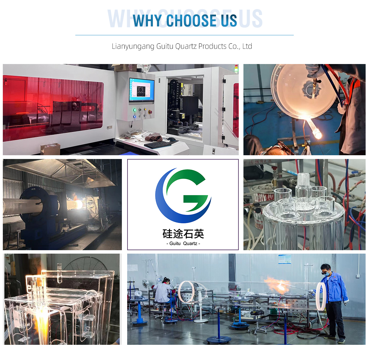
Lianyungang Zelvo Quartz Products Co., Ltd. is a specialized high-purity quartz manufacturer located in Donghai County, Jiangsu Province – the celebrated crystal capital of China that supplies the raw material backbone for the nation's advanced optics and semiconductor sectors. Our industrial footprint integrates optical-grade fused silica plate manufacturing, sapphire wafer polishing, high-purity quartz tubing, CVD wafer boats, and precision laboratory instruments under one rigorous quality system.
Our true competitive differentiator lies in high-precision micro-machining and advanced surface treatment: laser slotting, multi-axis grooving, CNC milling, ultrasonic hole drilling, high-temperature flame annealing, and proprietary cleanroom acid cleaning. Backed by senior glass engineers with over 10 years of hands-on semiconductor quartz manufacturing experience, we offer comprehensive DFM (Design for Manufacturability) advice before the first cut is made.
Every critical furnace tube, wafer boat, and etch ring undergoes rigorous in-process verification before clean packaging.
Raw silica boules and tubes are tested for visual bubble classification, seed inclusions, and structural striae per strict semiconductor standards.
High-precision 5-axis CNC diamond grinding and cold laser slotting cut complex wafer carrier geometries with tight tolerances down to ±0.05 mm.
Master glassblowers perform hydrogen-oxygen torch welding, followed by controlled cycle electric annealing at 1215 °C to eliminate thermal stress.
Ultra-pure HF/HNO₃ chemical etching dissolves subsurface mechanical micro-fissures, followed by 18.2 MΩ-cm DI water ultrasonic purging.
Coordinate Measuring Machine (CMM) dimensional verification, particle inspection, double vacuum PE bagging, and heavy-duty suspension crating.
Direct technical answers to the most common queries raised by cleanroom fab managers, equipment engineers, and international procurement leaders.
Real-world glimpses into our workshop, precision glassblowing lathes, and finished semiconductor fused quartz ware components.
 Semiconductor Quartzware Family
 5-Axis CNC Micromachining
 Stress-Free Laser Slotting
 Front-End Fab Compatibility
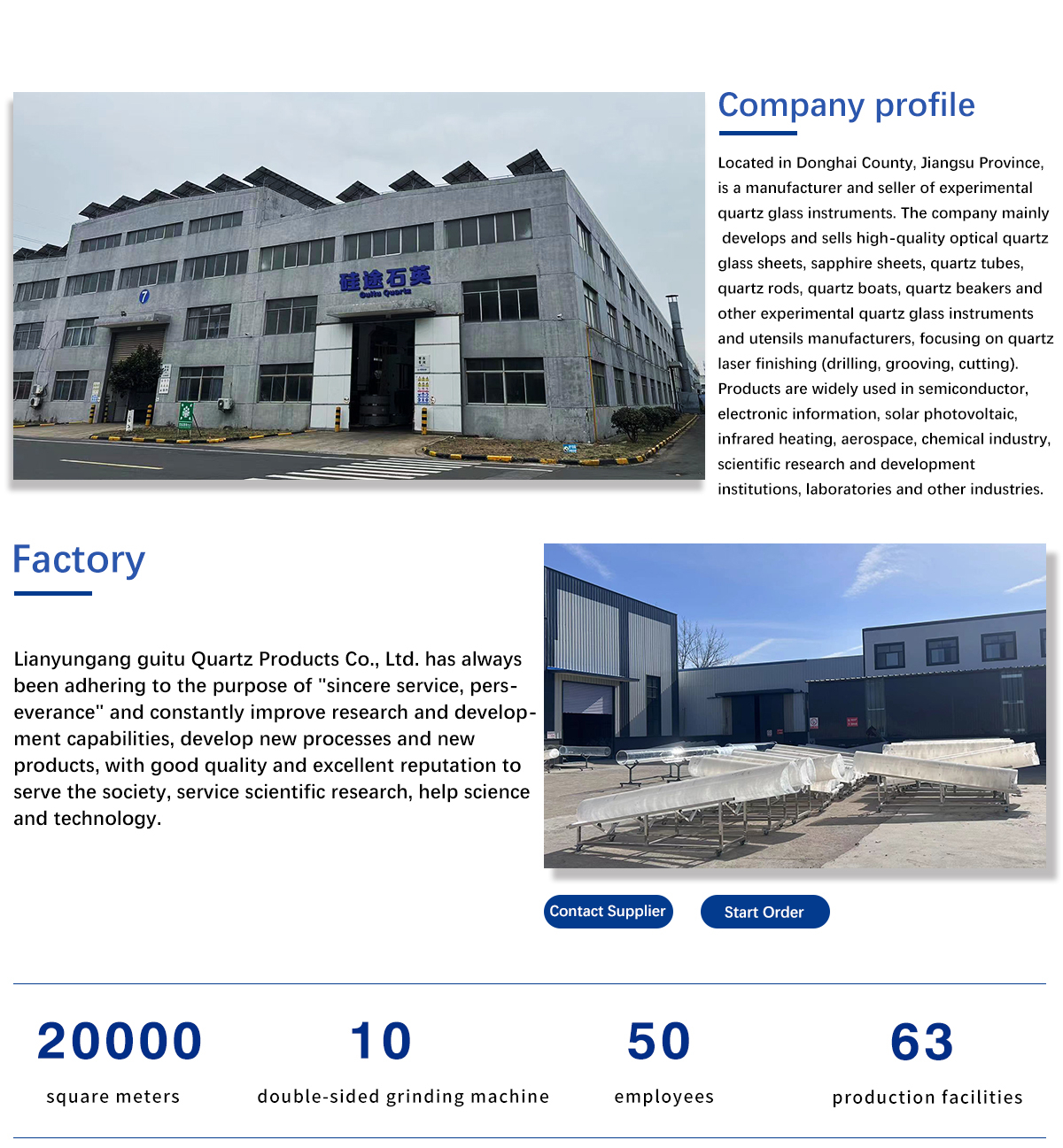 Donghai Manufacturing Hub
Lianyungang Zelvo Quartz Products Co., Ltd. – Semiconductor Fused Quartz Ware engineered to perfection in Donghai, Jiangsu.
 Coordinate Metrology (CMM)
 Diffusion Process Tubes
 Certified Optical Quality
 Cleanroom Export Packing
Send your CAD drawing, target operating temperatures, and wafer sizing parameters. Our senior quartz engineering team will review technical tolerances and respond within 2 hours with pricing and manufacturing lead time.
[email protected]