Featured Optical Quartz Blanks, Plates & Precision Components
Directly manufactured in Donghai, Jiangsu. Fully integrated production from synthetic fused silica slicing and laser trepanning to double-sided optical planarization and custom prism blank milling.
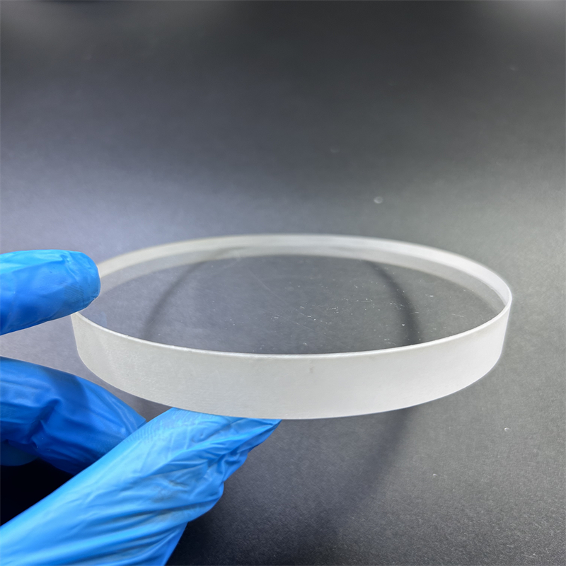
High-Temperature Transparent UV Quartz Glass Plate & Disc
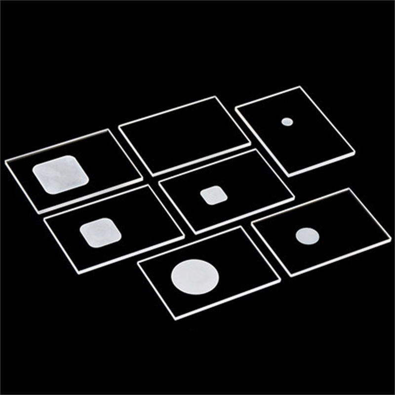
High Temperature Fused Quartz Sheet for XRD Sample Testing
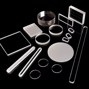
Custom Optical Grade Fused Transparent Quartz Sample Sheet
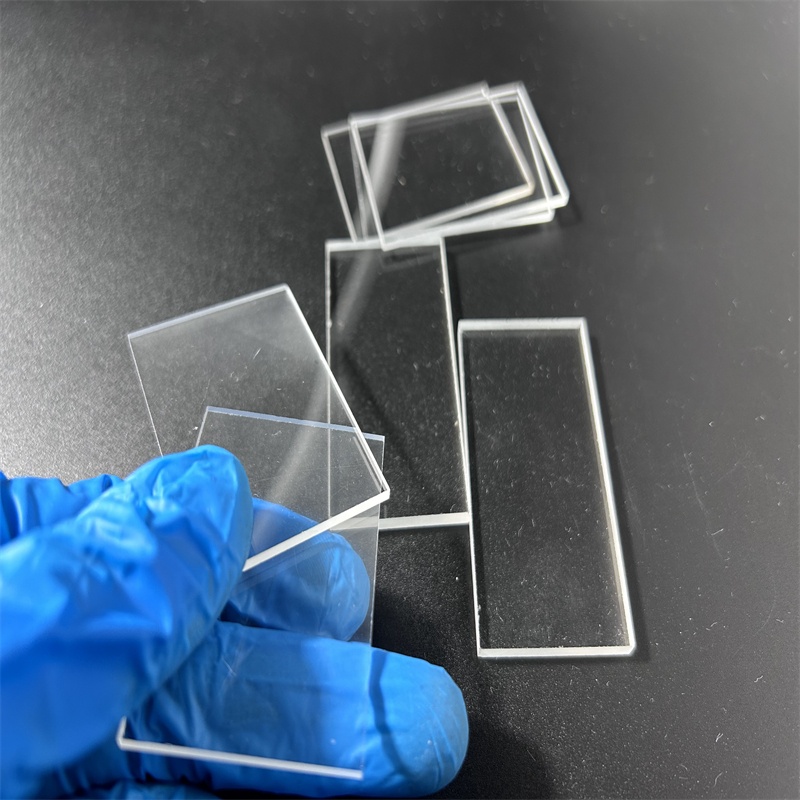
Customized Optics-Grade Transparent Quartz Clear Plate
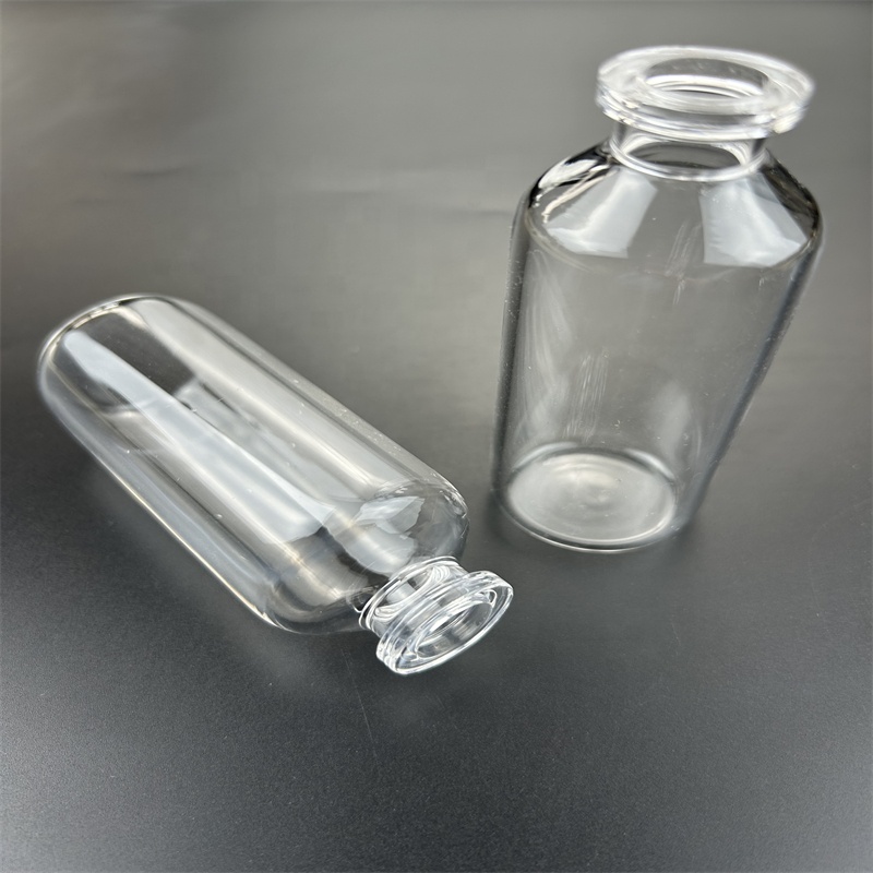
High-Pressure Ozone-Free Quartz Glass Ampoules
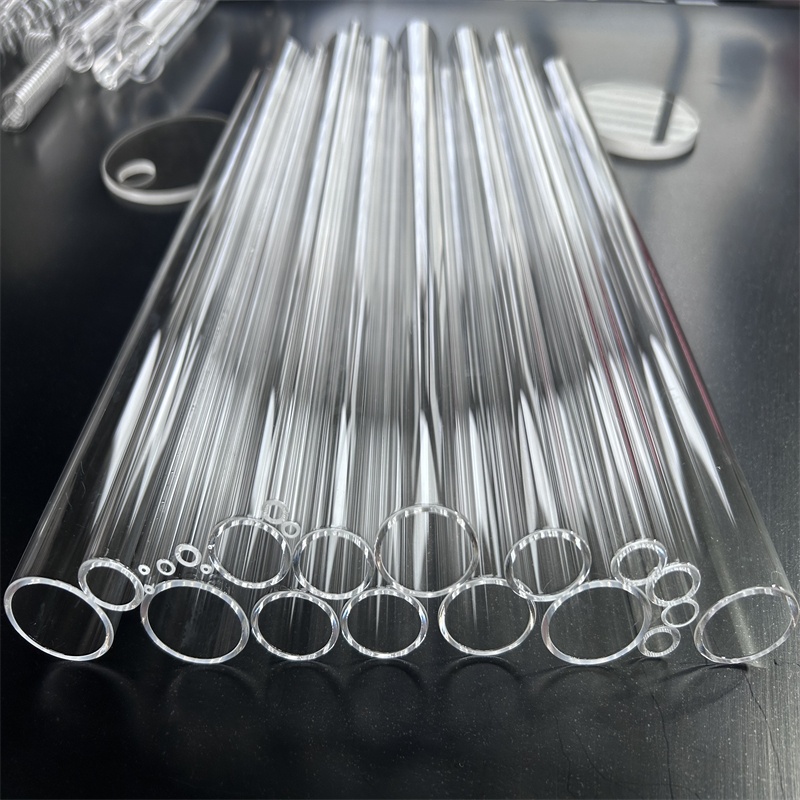
Clear 99.99% Pure Fused Quartz Twin Tube Assembly
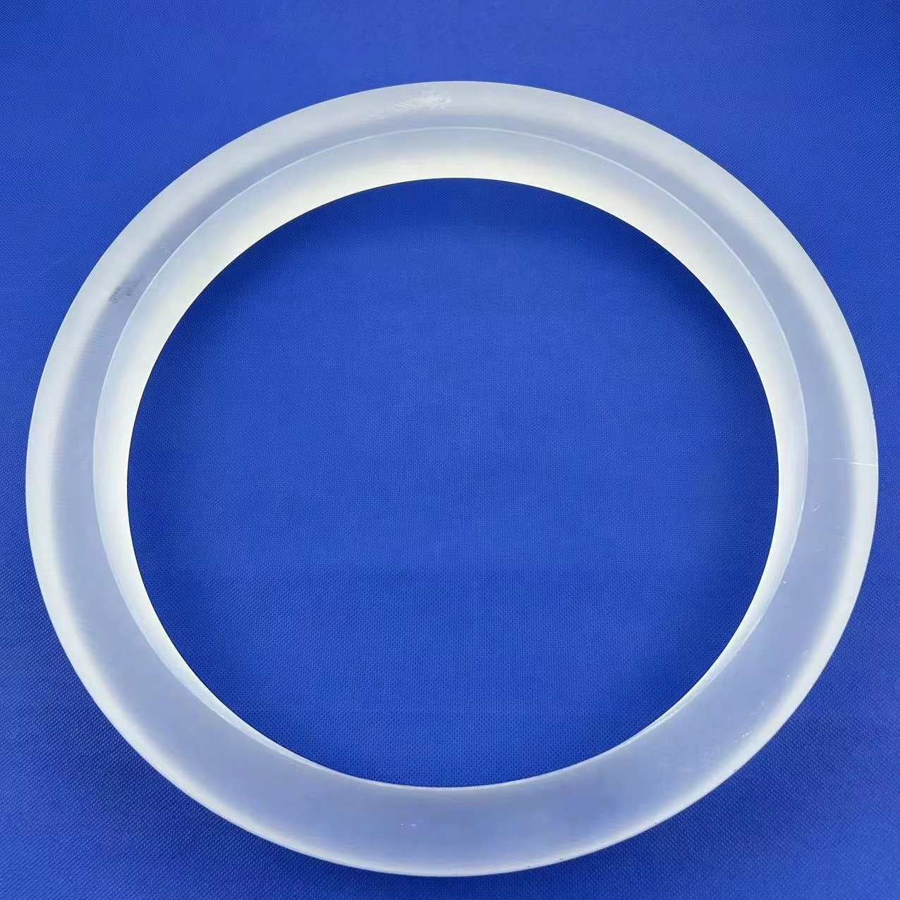
Custom Coated 99.99% Quartz Rings for Semiconductor CVD
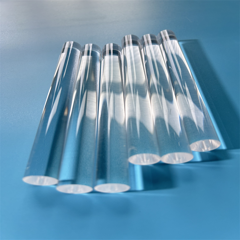
High-Purity Optical Quartz Light Guide Rod
Engineering Foundations of Precision Optical Quartz Prisms
A comprehensive metallurgical and optical analysis of substrate selection, wavefront transmission, geometric tolerance control, and laser-matter interaction in industrial fused silica prisms.
In modern optoelectronics, quantum photonics, and semiconductor lithography, the optical prism represents far more than an elementary refractive component. High-performance dispersion prisms, right-angle steering prisms, retroreflecting Porro/corner-cube prisms, Dove beam rotators, and Brewster-angle windows serve as fundamental building blocks where material homogeneity, bulk absorption, and surface micro-roughness dictate overall system fidelity. As international procurement leaders evaluate China top optical quartz prism factories and exporters, the decisive selection criteria have evolved past baseline unit costs toward verifiable material provenance, sub-nanometer surface integrity, and strict adherence to ISO 10110 drawing callouts.
1. Substrate Metallography & Grade Differentiation
Optical quartz components exported from China's primary manufacturing cluster in Donghai County, Jiangsu, fall into three standardized crystalline and synthetic amorphous categories. Selecting the incorrect grade results in instantaneous failure under ultraviolet radiation or deep-infrared absorption bands:
- JGS1 (Synthetic Fused Silica): Produced via the chemical vapor deposition (CVD) or flame hydrolysis of high-purity silicon tetrachloride (SiCl₄). Free of macroscopic bubbles, striations, and inclusions. Characterized by negligible trace metallic contamination (Fe < 0.05 ppm) and a controlled hydroxyl (OH⁻) content of 800 to 1200 ppm. It provides high optical transmission throughout the Deep Ultraviolet (DUV) band from 185 nm to 2500 nm, making it the premier choice for excimer laser prisms (193 nm, 248 nm) and fluorescence spectrophotometry.
- JGS2 (Fused Quartz / Electrically Fused Natural Crystal): Synthesized by melting ultra-high purity natural crystal quartz gravel inside high-temperature vacuum resistance furnaces. While displaying slightly higher internal micro-inhomogeneities than JGS1, JGS2 delivers broad spectral transmission from 220 nm to 2600 nm. It combines mechanical robustness, high chemical inertness, and a high continuous operating temperature threshold of 1100°C with an attractive price-to-performance ratio for thermal imaging, optical pyrometry, and visible-spectrum beam redirection.
- JGS3 (Infrared-Grade Water-Free Fused Silica): Engineered through gas-phase oxidation or vacuum degassing processes that purge residual water molecules, reducing hydroxyl content below 2 to 5 ppm. This effectively suppresses the destructive OH⁻ absorption band situated between 2600 nm and 2800 nm, rendering JGS3 the required substrate for mid-wave infrared (MWIR) beam paths, gas sensing filters, and Nd:YAG / Fiber laser delivery prisms operating at 1064 nm and above.
| Physical / Optical Parameter | JGS1 (DUV Synthetic) | JGS2 (Optical Fused) | JGS3 (IR Synthetic) | Borosilicate Crown (N-BK7) |
|---|---|---|---|---|
| Refractive Index ($n_d$ @ 587.6 nm) | 1.4585 | 1.4584 | 1.4585 | 1.5168 |
| Abbe Number ($V_d$) | 67.8 | 67.7 | 67.8 | 64.17 |
| Useful Spectral Range | 185 nm – 2500 nm | 220 nm – 2600 nm | 260 nm – 3600 nm | 330 nm – 2100 nm |
| Thermal Expansion Coeff. (0–300°C) | $5.5 \times 10^{-7} \text{ K}^{-1}$ | $5.5 \times 10^{-7} \text{ K}^{-1}$ | $5.5 \times 10^{-7} \text{ K}^{-1}$ | $7.1 \times 10^{-6} \text{ K}^{-1}$ |
| OH Content (ppm by weight) | 800 – 1200 | 150 – 200 | < 5 | N/A |
| Maximum Continuous Temp. | 1100 °C | 1100 °C | 1100 °C | ~450 °C |
| Softening Point | 1683 °C | 1680 °C | 1683 °C | ~710 °C |
| Laser Damage Threshold (1064nm, 10ns) | > 25 J/cm² | > 12 J/cm² | > 20 J/cm² | ~ 5 J/cm² |
2. Geometrical Precision, Surface Metrology & Tolerancing
Unlike standard window glass or tubular fluid conduits, precision optical prisms impose demanding geometric constraints. When laser beams reflect internally or refract across boundary interfaces, angular deviances cause significant pointing errors across extended optical path lengths. Premier Chinese optical fabrication facilities maintain cleanroom environments (ISO Class 6 / Class 7) and utilize advanced CNC double-sided planetary polishers alongside magneto-rheological finishing (MRF) to deliver standard and ultra-precision tolerances:
- Angular Deviation & Pyramid Error: Standard industrial prisms operate with angular errors within ±30 to ±60 arcseconds. For high-precision metrology, LiDAR, and analytical spectrometer systems, Zelvo Quartz and top-tier domestic manufacturers utilize laser collimator and autocollimator goniometers to restrict angular error to < 3 arcseconds, with pyramid errors held below 1 arcminute.
- Surface Figure / Wavefront Distortion (Flatness): Measured interferometrically at the He-Ne laser baseline wavelength (632.8 nm). Standard production tiers maintain $\lambda/4$ per surface, whereas high-grade laser prisms achieve $\lambda/10$ to $\lambda/20$ peak-to-valley across the clear aperture ($>90\%$ of physical area), preventing phase distortion in coherent optical systems.
- Surface Quality (Scratch-Dig per MIL-PRF-13830B & ISO 10110): Optical surfaces exposed to high peak-power pulsed beams require strict scratch-dig ratings of 20-10 or 10-5 to eliminate localized electric field intensification. Routine industrial inspection relies on darkfield microscopy and automated surface defect mappers.
- Sub-Surface Damage (SSD) Suppression: Traditional aggressive grinding leaves microscopic micro-cracks below the polished optical layer, which act as thermal stress risers and laser-damage initiation sites. Modern chemical-mechanical polishing (CMP) utilizing colloidal silica slurries ensures the complete removal of the Beilby layer, achieving a surface micro-roughness ($Ra$) below 0.3 nm (super-polished).
Why Global Procurement Teams Partner with Zelvo Quartz
Based in Donghai County, Jiangsu—China's crystal capital—we combine localized raw silica supply chains with advanced CNC optical machining and certified export frameworks.
Direct Origin Sourcing
Located in Donghai, Jiangsu, the global processing hub for 99.99% SiO₂ quartz. We bypass intermediate traders to ensure raw blank homogeneity, cost stability, and complete material traceability.
CNC Laser & Flame Machining
Full custom drawing-based fabrication: CNC 5-axis grinding, ultrasonic drilling, deep-hole trepanning, optical flame polishing, slotted XRD grooving, and structural quartz tube bending.
1-Piece MOQ Prototyping
Eliminate trial bottlenecks. We support experimental laboratories, universities, and high-tech startups with 1-piece custom prototyping, ramping to thousands of units for production runs.
Shockproof Global Logistics
Multilayer shock-absorbing packaging (vacuum-sealed cleanroom bags, customized high-density foam, certified export timber crates). FOB, CIF, DDP, and door-to-door express delivery.
Future Procurement Trends for Optical Quartz Prisms (2025–2030)
Strategic supply chain dynamics, technological disruption, and shifting compliance frameworks driving international sourcing decisions over the next five years.
Surging Demand in DUV/EUV Semiconductor Lithography
Direct-to-Factory Engineering Integration (Bypassing Tiers)
Extreme Laser Damage Threshold (LIDT) Standardisation
Technological Advancements in Quartz Prism Manufacturing
How Chinese optical factories are adopting Ion Beam Figuring (IBF), atomic-scale planarization, and advanced metrology to meet tight optical tolerances.
The global precision optics landscape is experiencing a rapid technological transition. Traditional mechanical pitch polishing and manual goniometric adjustment, while historically reliable, are no longer sufficient to satisfy the angular tolerances (< 1 arcsec) and surface figures ($\lambda/20$) required by aerospace navigation gyroscopes, space-based optical communications, and quantum entanglement experiments. Top-tier manufacturers in China are executing major technical upgrades across several primary domains:
1. Deterministic Micro-Finishing: Ion Beam Figuring (IBF) & MRF
To transcend the physical limits of contact-based polishing pads, high-end fabrication shops have introduced Magneto-Rheological Finishing (MRF) and Ion Beam Figuring (IBF). MRF utilizes a magnetically stiffened polishing ribbon to predictably buff out mid-spatial frequency errors without inducing edge roll-off on right-angle and equilateral prisms. For final corrective passes, vacuum IBF bombards the fused quartz substrate with accelerated argon ions, milling away sub-nanometer topographical peaks at atomic scale. This deterministic approach enables volume manufacturing of prism wavefront distortions below $\lambda/20$ PV, while maintaining surface roughness $Ra < 0.2$ nm.
2. Advanced Thin-Film Dielectric Deposition
A precision quartz prism is frequently defined by its coating. Conventional thermal evaporation methods yield porous thin films that suffer from spectral shifts due to environmental humidity absorption. Modern Chinese export facilities employ Ion-Assisted Deposition (IAD) and Ion Beam Sputtering (IBS) within high-vacuum cleanrooms. These high-energy plasma processes pack dielectric oxide layers (e.g., SiO₂, Ta₂O₅, HfO₂, Al₂O₃) with bulk-like packing densities, enabling:
- Ultra-Broadband Anti-Reflective (BBAR) Coatings: Typical reflection loss per surface minimized to $R < 0.2\%$ across the visible or NIR spectrum.
- High-Efficiency Polarizing Beam Splitter (PBS) Coatings: Extinction ratios exceeding $T_p/T_s > 1000:1$ for laser separation systems.
- High-Reflectivity Dielectric Cavity Coatings: Internal reflection surfaces optimized to $R > 99.95\%$ for laser cavity ring-down spectrometers.
3. Full-Aperture Absolute Metrology Systems
Quality assurance protocols have shifted from sampling-based inspection to 100% digital data logging. Modern facilities integrate phase-shifting Fizeau laser interferometers (Zygo Verifire or equivalent), non-contact 3D optical profilometers, and dual-axis high-speed photo-electric autocollimators. Buyers receive comprehensive verification packages with every export shipment, including interferometric wave-front phase maps, MTF (Modulation Transfer Function) charts, spectrometer transmission curves from 190 nm to 3200 nm, and coordinate measuring machine (CMM) dimensional verification sheets.
Frequently Asked Questions for International B2B Buyers
Clear, engineering-backed answers addressing the most common technical, logistical, and commercial inquiries encountered when sourcing quartz optics from China.
What is the practical difference between Natural Fused Quartz and Synthetic Fused Silica for optical prisms?
What angular and dimensional tolerances can your workshop reliably maintain?
How do you test and certify Laser Damage Threshold (LIDT) for high-power laser prisms?
Can you provide custom anti-reflective (AR) or high-reflection (HR) coatings on fused quartz prisms?
What is your Minimum Order Quantity (MOQ) and rapid prototyping lead time?
How do you package fragile optical quartz prisms to prevent transit damage and surface degradation?
Which international trade terms (Incoterms) and payment methods do you support?
Request an Optical Engineering Review & Quotation
Send us your optical drawings, required dimensions, tolerances, substrate grade (JGS1, JGS2, JGS3), and quantity. Our senior optical fabrication engineers will review manufacturability, verify tolerances, and provide an itemized quote within 2 hours.