Featured OEM/ODM Fused Silica & Quartz Components
Directly sourced from our Lianyungang manufacturing lines, these components represent our core custom-fabrication competencies for semiconductor fabrication, thermal diffusion furnaces, analytical spectroscopy, and corrosive chemical reactors.
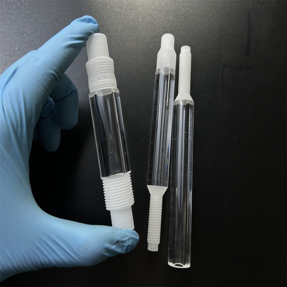
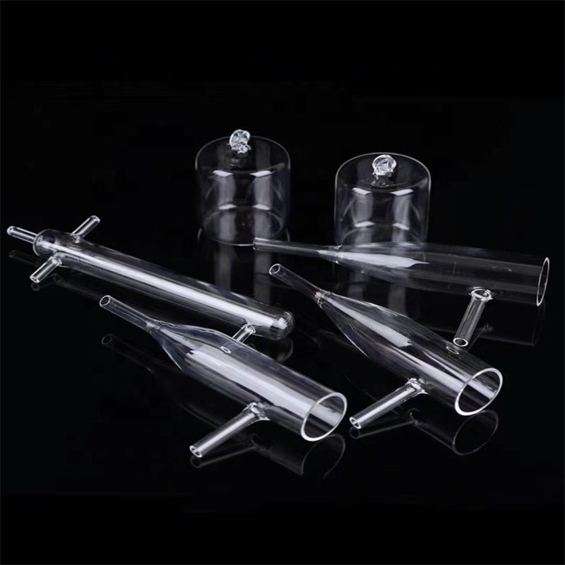
Customized High Purity Threaded Transparent UV Quartz Glass Tube
Engineered for deep-ultraviolet (DUV) photochemical exposure and pressurized line interfaces. Features optical flame-polished thread finishes and custom bending tolerances.
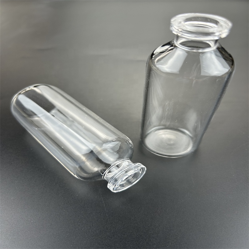
Custom High Pressure Ozone-Free Quartz Glass Ampoules
Hermetically sealable, chemical-resistant quartz glass ampoules providing non-reactive sample isolation under aggressive autoclave and cryogenic thermal regimes.
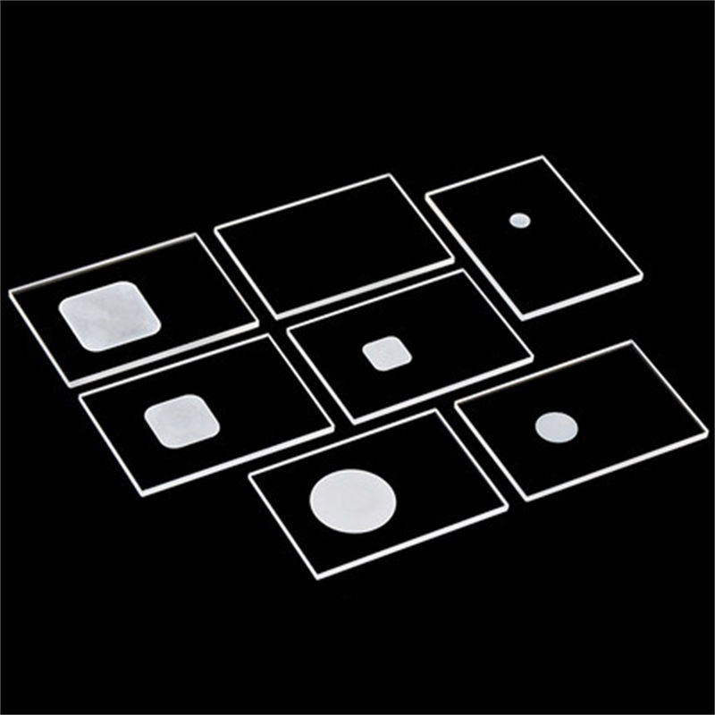
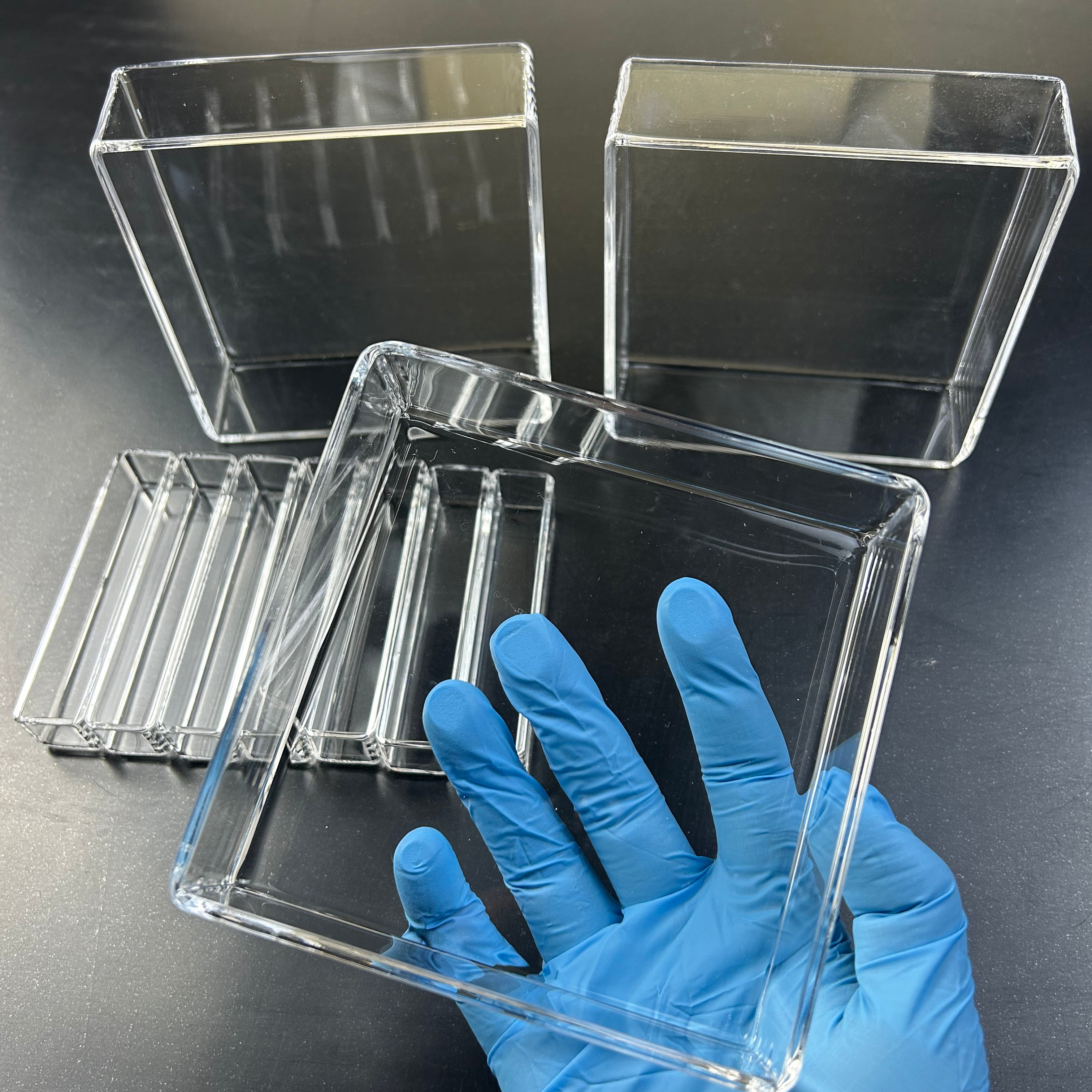
High Temp Fused Quartz Glass Sheet for XRD Testing Tank
Zero-diffraction background sample carriers customized with CNC precision slotted channels, providing superior planar dimensional consistency during high-temperature X-ray analysis.
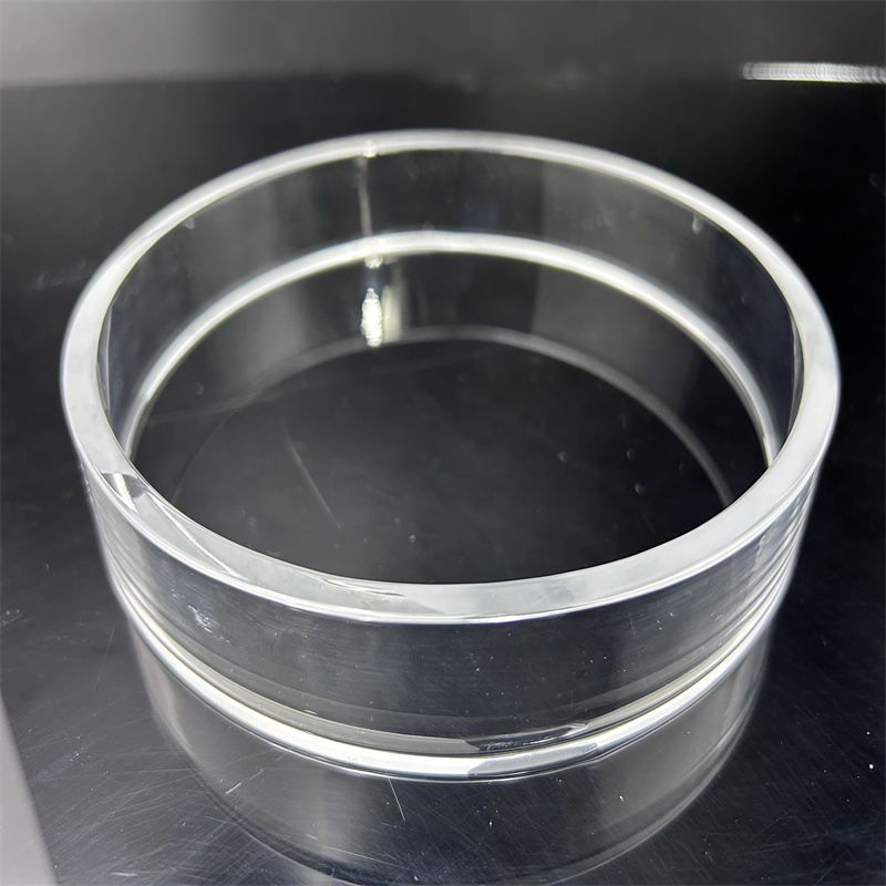
High Transparent Corrosion-Resistant Fused Quartz Bell Jar
Engineered for semiconductor wafer etching and physical vapor deposition. Demonstrates extreme resistance to fluorine and chlorine-based reactive plasmas under vacuum.
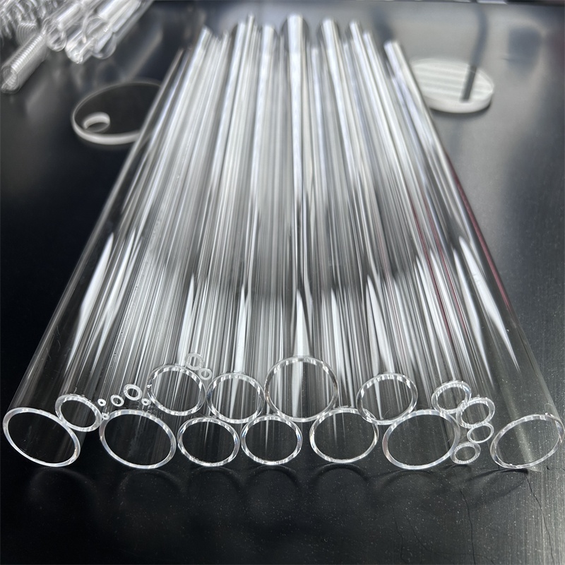
Clear Laboratory High Temp Twin Tube for CVD Furnaces
Dual-bore furnace reactor tube manufactured with precision welding for multi-gas thermal CVD systems, eliminating cross-flow thermal gradients and enabling isolated reactant routing.
Customized Fused Quartz Glass Circular Cylinder Crucible Tank
Heavy-wall fused silica crucibles engineered for rare earth melting, metallurgical reduction, and polysilicon synthesis. Thermal shock immune with near-zero thermal expansion.
High Temp 99.99% Pure Fused Quartz Twin Tube with Bending
Designed for twin-filament infrared emitters and high-density heating modules. Engineered with gas-tight welding and precision center-to-center bore consistency.
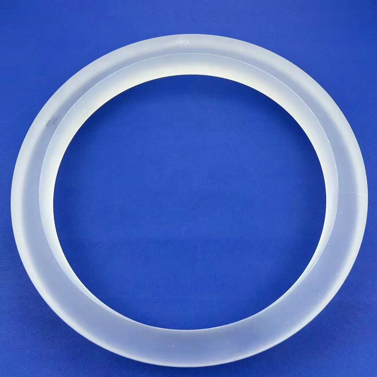
Custom Coated 99.99% Pure Quartz Rings for Semiconductor CVD
Precision lapped and chemically coated containment rings for wafer clamp Chucks and CVD process chambers. Delivers exceptional mechanical stability and minimal particle shedding.
Material Science: Fused Silica vs. Fused Quartz Engineering Profiles
Understanding the thermal thermodynamics, spectral transmission profiles, and impurity budgets is critical for procurement managers specifying fused silica components in high-stress operational environments.
In precision engineering, the nomenclature between fused silica (synthetically generated via gas-phase chemical oxidation of silicon precursors such as SiCl₄) and fused quartz (thermally melted from natural high-purity crystalline quartz rock) defines functional boundaries. While both consist predominantly of amorphous silicon dioxide (SiO₂), synthetic fused silica exhibits ultra-low metallic trace contamination (sub-ppb levels) and superior deep-ultraviolet (DUV) transmission down to 185 nm. Conversely, electric-arc melted fused quartz delivers unmatched dimensional structural rigidity, superior resistance to high-temperature sag at temperatures exceeding 1150°C, and minimal hydroxyl (OH) absorption, making it the globally preferred substrate for semiconductor furnace process tubes and diffusion chambers.
Thermodynamic & Physical Constants
| Physical Parameter | Nominal Value | Test Standard |
|---|---|---|
| Density (ρ) | 2.20 ± 0.01 g/cm³ | ASTM C693 |
| Continuous Working Temp | 1100 °C | DIN 52324 |
| Max Peak Service Temp | 1300 °C (< 2 hrs) | DIN 52324 |
| Softening Point (η = 10^7.6 dPa·s) | 1683 °C | ASTM C338 |
| Annealing Point (η = 10^13.0 dPa·s) | 1215 °C | ASTM C336 |
| Strain Point (η = 10^14.5 dPa·s) | 1070 °C | ASTM C336 |
| Thermal Expansion Coeff (CTE) | 5.5 × 10⁻⁷ /K (20–320°C) | ASTM E228 |
| Dielectric Constant (1 MHz) | 3.75 | ASTM D150 |
Note: Values represent typical production averages for electronic-grade clear fused quartz. Batch inspection certificates (CoA) are supplied with commercial deliveries.
Trace Element Impurity Profile (ICP-MS)
| Trace Element | Element Symbol | Standard Grade (ppm) | Semiconductor (ppm) |
|---|---|---|---|
| Aluminum | Al | 14.0 – 18.0 | < 8.0 |
| Iron | Fe | 0.15 – 0.30 | < 0.05 |
| Titanium | Ti | 1.0 – 1.8 | < 0.5 |
| Calcium | Ca | 0.4 – 0.8 | < 0.3 |
| Magnesium | Mg | 0.05 – 0.1 | < 0.03 |
| Sodium + Potassium | Na + K | 0.5 – 1.2 | < 0.2 |
| Lithium | Li | 0.2 – 0.6 | < 0.1 |
| Hydroxyl (OH⁻) | OH | < 20 (Dehydroxylated) | < 5 (Dry Electrically Fused) |
Low alkali metal (Na, K, Li) concentrations prevent ionic migration into silicon wafer lattices during high-temperature gate oxide growth.
End-to-End Precision Quartz Processing Capabilities
From raw drawn quartz ingot extrusion to complex 5-axis CNC machining and high-purity glassblowing, our workshop integrates traditional flame artistry with modern computerized automation.
Laser Micro-Drilling & Trepanning
CO₂ and picosecond laser drilling achieving micro-apertures down to Ø 0.15 mm without micro-cracking, thermal chipping, or surface flaking along bore perimeters.
CNC Ultrasonic Grooving & Slotting
Diamond-tooled ultrasonic machining for wafer carrier boats, microfluidic channel engraving, and slotted XRD tanks with positioning repeatability of ±0.005 mm.
Precision Flame Bending & Coiling
Hydrogen-oxygen lathe manipulation for seamless U-bends, multi-turn cooling coils, and twin-bore geometry without wall thinning, bubbling, or oval distortion.
Optical Fire & Lap Polishing
Double-sided planetary lapping achieving surface roughness Ra < 0.5 nm, parallelisms under 10 arcseconds, and optical scratch-dig specifications of 20-10 or 10-5.
High-Vacuum Flange Fusion
Gas-tight fusion welding of standard ISO-KF, CF, and ground spherical taper joints directly onto fused silica tube bodies, certified to helium leak rates < 1×10⁻⁹ mbar·l/s.
Annealing & Chemical Dehydroxylation
Controlled electric furnace annealing cycles up to 1215°C eliminate residual mechanical stress, followed by hydrofluoric acid etching and 18.2 MΩ·cm DI water cascades.
Future Sourcing & Technological Trends in Fused Silica
Critical insights for procurement directors forecasting the 2025–2030 semiconductor node migrations, clean energy demands, and photonic integration shifts.
Lianyungang Zelvo Quartz Products Co., Ltd.
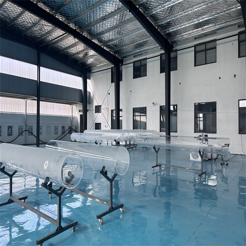
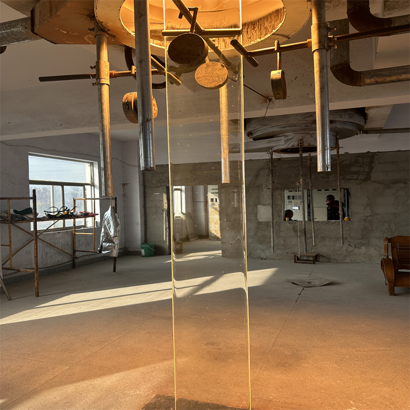
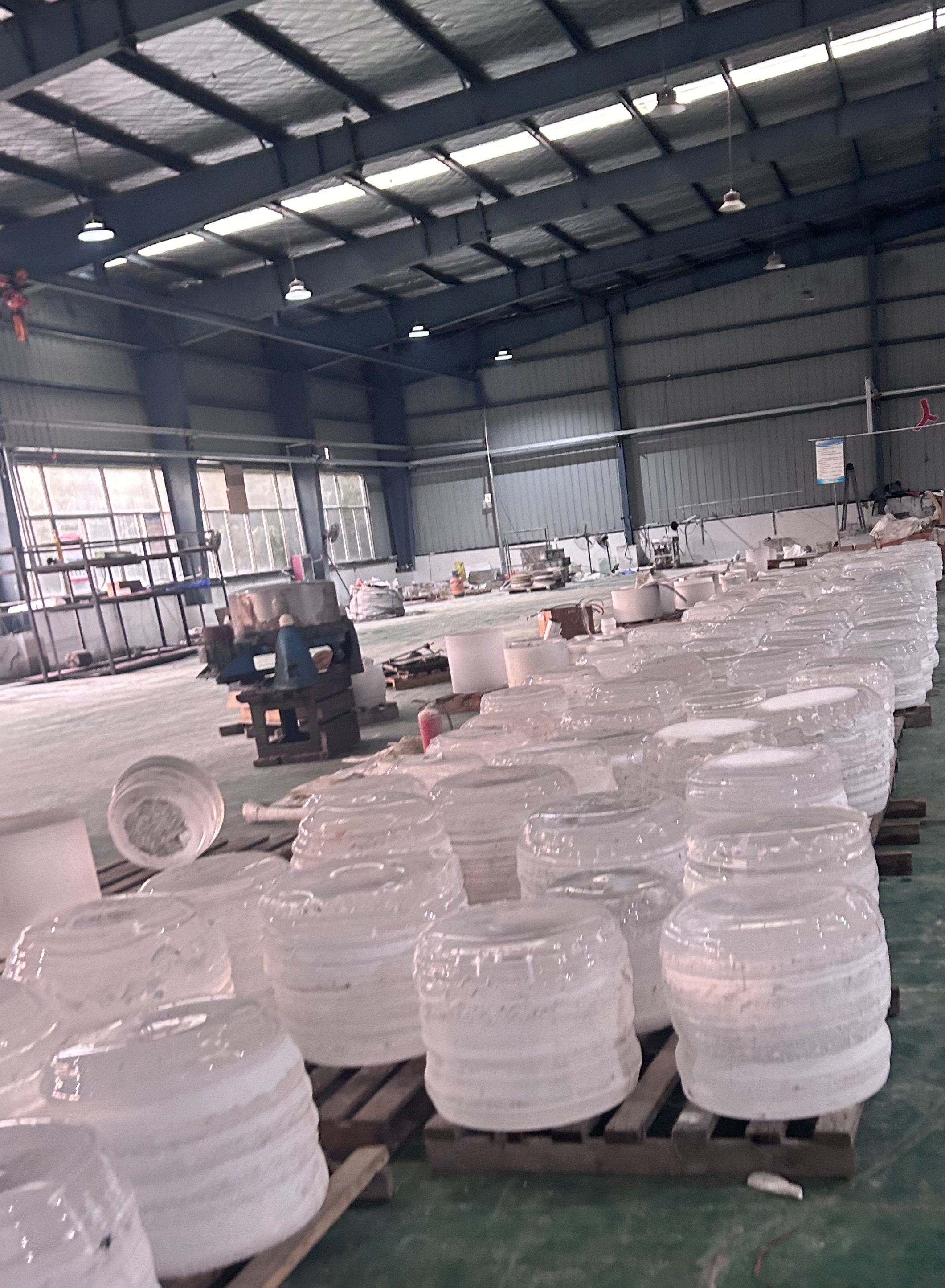
Headquartered in Donghai County, Jiangsu Province—globally celebrated as the "Crystal Capital of China"—Zelvo Quartz sits directly at the epicenter of the world's most concentrated natural silica extraction, purification, and engineering ecosystem. We integrate natural raw material control, gas-flame extrusion, and high-precision secondary machining under one continuous ISO 9001-certified roof.
Our technical directors possess over a decade of dedicated expertise solving thermal strain, devitrification, and vacuum seal challenges for clients across North America, Southeast Asia, South America, and Europe. Whether you require standard 10-piece BET consumable tubes or a complex one-off semiconductor quartz bell jar with integrated sensor wells, our agile production setup guarantees unmatched speed and dimensional compliance.
- Onsite-Verified Manufacturing Facility
- 100% Engineering Review Within 2 Hours
- MOQ Starting from Just 1 Piece
- Class 10,000 Cleanroom Packaging
- Full Traceability & CoA Test Reports
- Global DDP, CIF & Express Door Logistics
Total Cost of Ownership (TCO) in Fused Silica Procurement
Analyzing purchase price against devitrification cycles, maintenance shutdowns, and catastrophic thermal fracture risk.
Experienced optical and semiconductor procurement engineers evaluate quartz suppliers through a Total Cost of Ownership (TCO) matrix rather than unit initial cost. A low-cost quartz furnace tube produced with substandard raw quartz sand will show elevated alkali contaminants (Na, K, Li > 2.5 ppm). At furnace operating temperatures above 1000°C, these alkali ions act as mobile nucleation centers, catalyzing rapid cristobalite devitrification. Cristobalite undergoes an aggressive volumetric contraction of approximately 5% during cool-down transitions across the 200–270°C phase inversion threshold, resulting in spontaneous catastrophic wall fracturing, loss of vacuum integrity, and ruined semiconductor wafer lots.
Devitrification Retardation
By strictly enforcing alkali limits (< 0.2 ppm Na+K) and optical surface flame-polishing, Zelvo quartz tubes suppress cristobalite formation, extending operational service life by 40% to 65% in continuous 1100°C furnace runs.
Precision Flange Seal Integrity
Out-of-flatness on flanged quartz bodies forces overtightening of mating collars, inducing high mechanical bending moments. Our computer-controlled lapping keeps flange flatness within < 0.02 mm, preventing assembly breakage.
Zero-Breakage Packaging Protocol
Engineered shock-absorbing EPE multi-layer tailored foams, suspension cradles, and heavy plywood crating compliant with ISPM-15 reduce international transit breakage claims to less than 0.12% across over 45 export destinations.
Technical & Sourcing Inquiries Answered
Critical engineering criteria, tolerance standards, and logistics policies for B2B buyers.
What is the standard purity of your fused silica and fused quartz tubes?
What dimensional tolerances can your machining and drawing facilities achieve?
Can you manufacture custom quartz parts directly from customer CAD drawings?
What is the operational thermal threshold of your quartz tubes, and how can devitrification be prevented?
What is your minimum order quantity (MOQ) and production sample lead time?
What shipping arrangements, trade terms, and safety packaging protocols do you maintain?
Request an Engineering Drawing Review & Quote
Send us your specifications, 2D/3D CAD drawings, or custom tolerance requirements. Our engineering team in Donghai will review your design, verify manufacturing feasibility, and deliver an official quotation within 2 hours.