Featured Quartz Components & Precision Plates
Precision-machined from ultra-pure quartz crystal ingots. Supporting 1-piece custom prototyping, ultrasonic drilling, laser micro-slitting, and optical double-sided polishing.
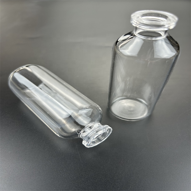
Custom High Pressure Corrosion Resistant Transparent 99.99% Pure Ozone Free Quartz Glass Ampoules
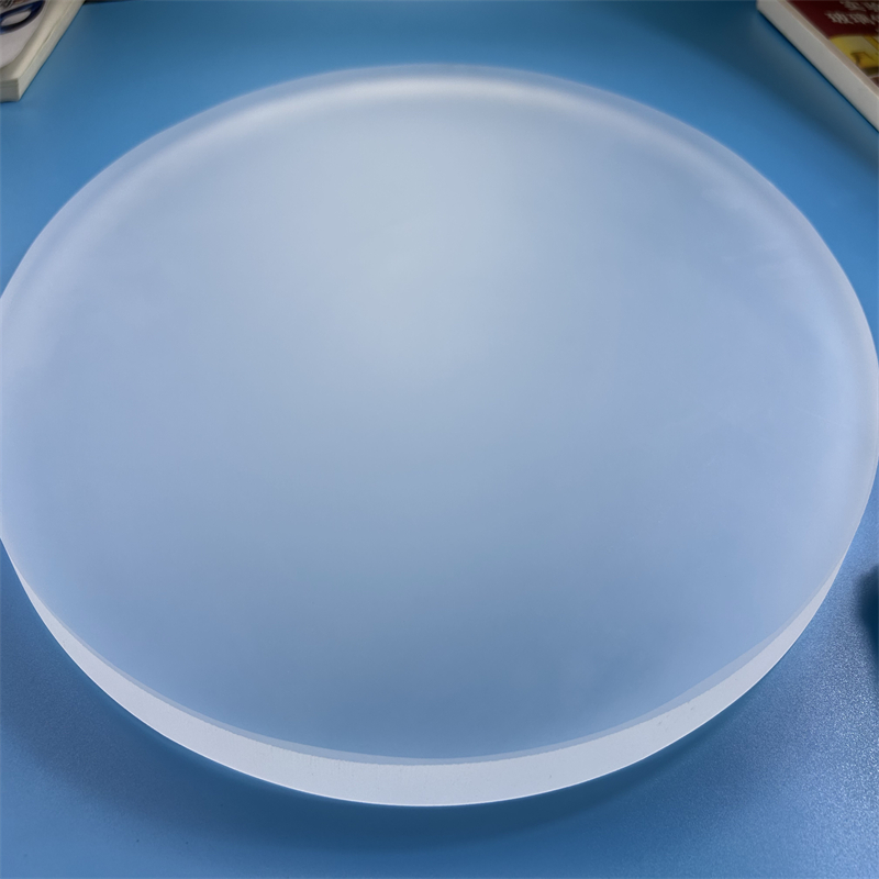
High Temperature Resistance Frosted Quartz Disc/Plate Semiconductor Applications Fused Quartz
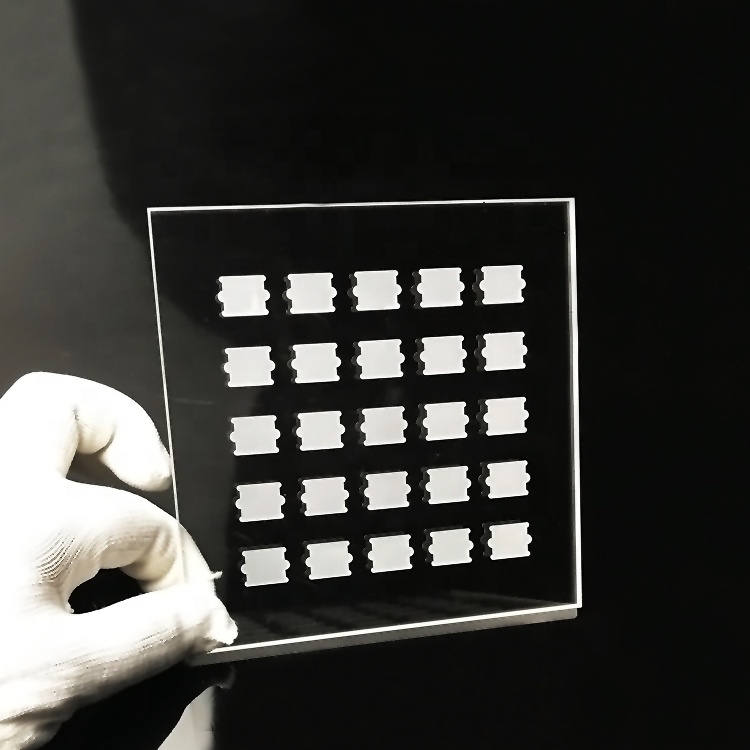
Factory Custom Fused Quartz Glass Circular High Temperature XRD Sample Holder
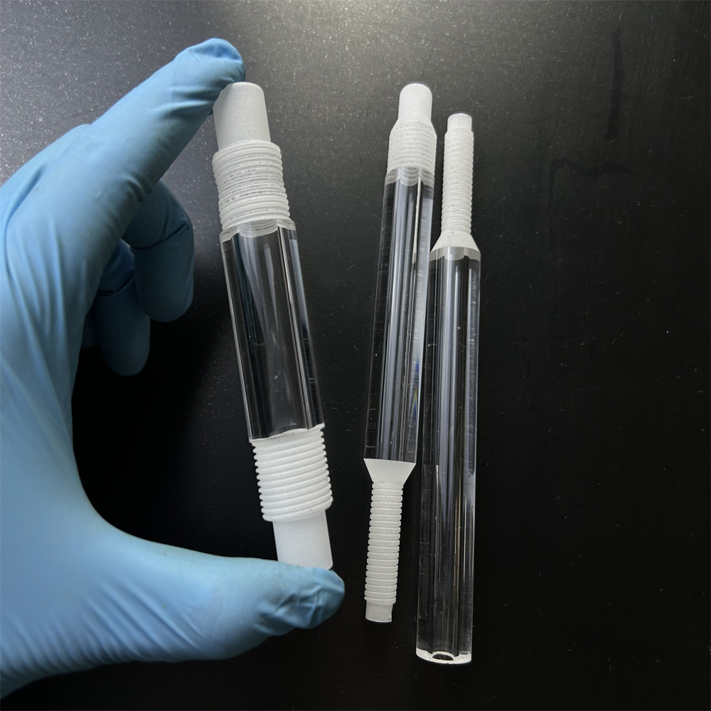
Customized High Purity Threaded Transparent UV Quartz Glass Tube Moulding Services
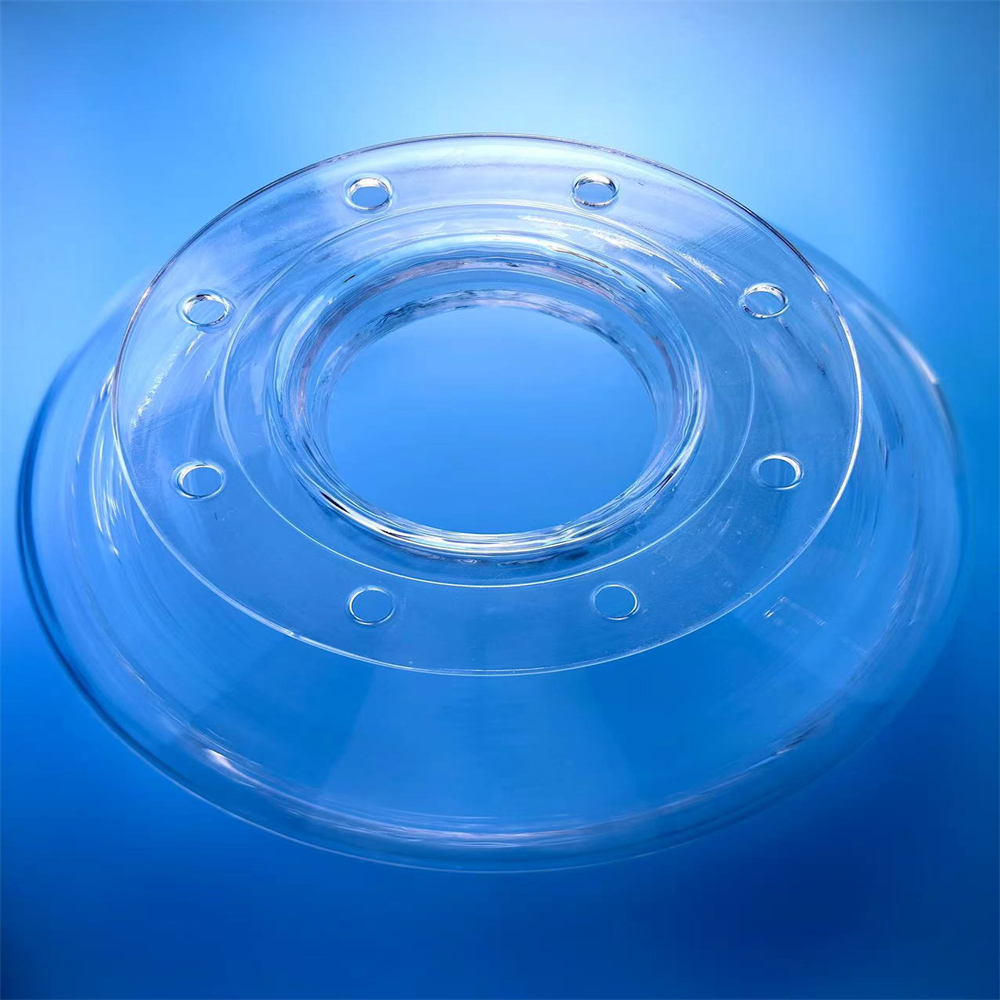
Customize Size Thickness Twin Tube Clear High Purity Flange Quartz Tube Fused Silica Ring
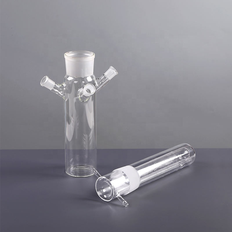
Customized High-Purity Quartz Glass Reactor Container Photocatalytic Degradation Vessel
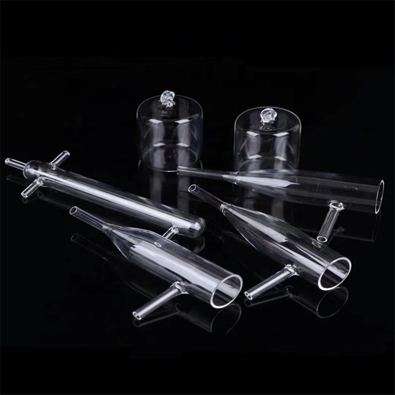
Custom Clear Laboratory High Temperature Twin Tube 99.99% Pure CVD Furnace Tube
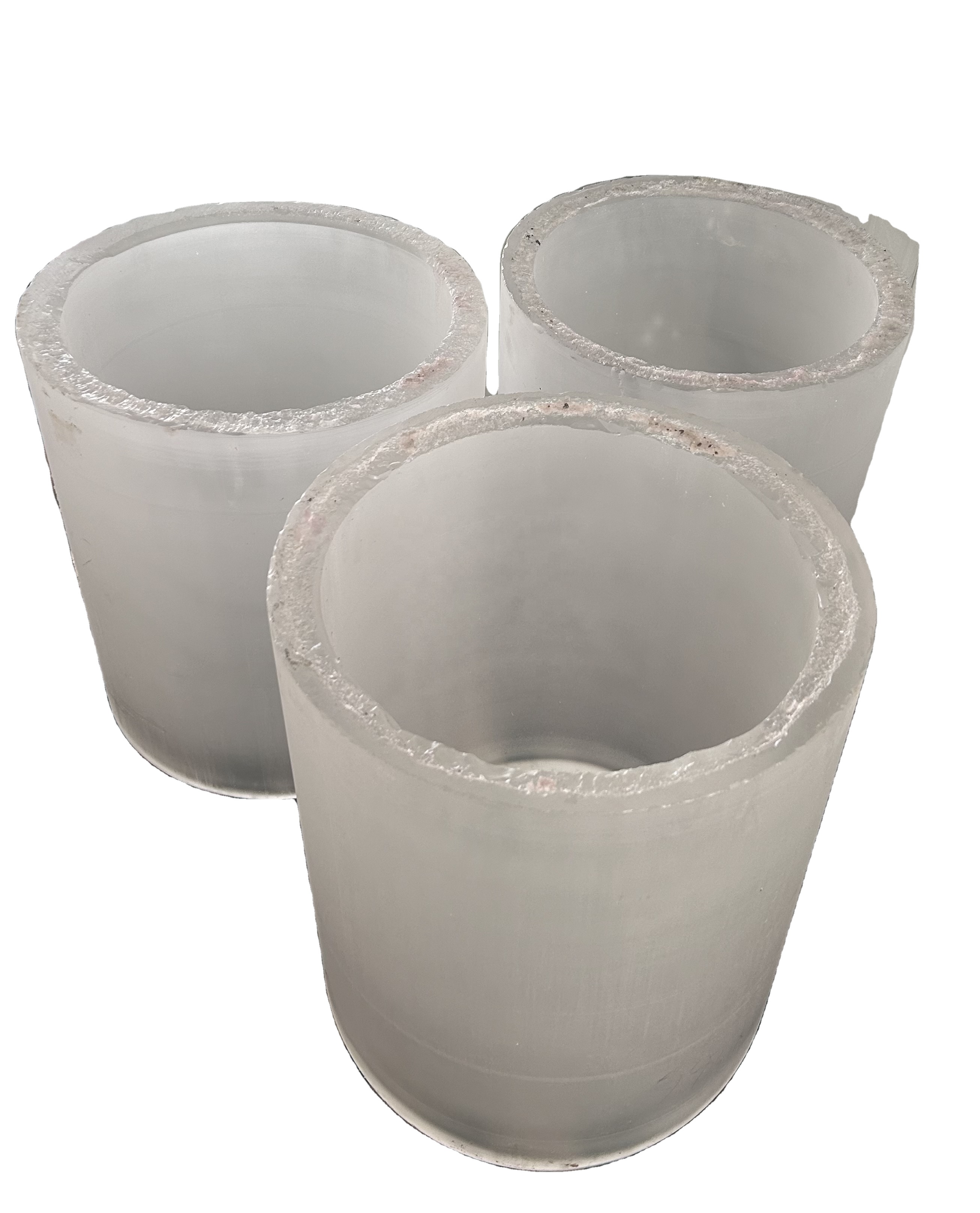
Open Ended Fused Quartz Frosted Glass Cylinder Ingot Moulding Welding Cutting Services
Engineering Whitepaper: The Critical Role of High-Purity Quartz Carrier Plates
In advanced microelectronics, compound semiconductor fabrication (GaN, SiC, GaAs), and sub-micron optical photolithography, wafer processing yields are profoundly contingent upon the thermo-mechanical stability and chemical inertness of handling fixtures. Quartz Carrier Plates (also known as fused silica carrier substrates, wafer handling platters, or XRD sample trays) represent an indispensable class of high-temperature tooling. Operating under extreme thermal gradients (up to 1100°C continuous regime) and highly corrosive plasma etching chemistries (including halogenated radicals), these plates provide the rigid, non-reactive foundation necessary to prevent wafer warpage, crystallographic slip, and trace metal contamination.
1. Material Physics: Natural Fused Quartz vs. Synthetic Fused Silica
Engineers sourcing carrier substrates must carefully discern between electrically fused natural quartz (commonly classified under JGS2/JGS3 standards) and chemical vapor deposition synthetic fused silica (JGS1 standard). Natural fused quartz, refined from high-purity natural silica sand in Donghai County, offers supreme structural rigidity, zero crystalline boundaries, and exceptional creep resistance at temperatures approaching the annealing point of 1215°C. For ultraviolet laser inspection, DUV wafer bonding, and direct optical alignment, synthetic silica provides near-zero bubble inclusion (Class 0 per DIN 3140) and deep UV transmission extending down to 185 nm.
| Physical / Thermal Property | Fused Quartz Carrier Plate | Borosilicate Glass | High-Purity Alumina (Al₂O₃) | Silicon Carbide (SiC) |
|---|---|---|---|---|
| Chemical Composition | ≥ 99.99% SiO₂ | ~81% SiO₂, 13% B₂O₃ | 99.5% - 99.9% Al₂O₃ | Sintered / CVD SiC |
| Density (g/cm³) | 2.20 | 2.23 | 3.92 | 3.15 |
| Max Continuous Temperature | 1100 °C (1300 °C Peak) | 450 °C | 1600 °C | 1450 °C |
| Coefficient of Thermal Expansion (CTE) | 0.54 × 10⁻⁶ / K | 3.3 × 10⁻⁶ / K | 7.2 × 10⁻⁶ / K | 4.0 × 10⁻⁶ / K |
| Thermal Shock Resistance | Exceptional (ΔT > 1000°C to H₂O) | Moderate (ΔT ≈ 150°C) | Poor (ΔT ≈ 200°C) | High (ΔT ≈ 400°C) |
| Dielectric Constant (1 MHz) | 3.75 (Extremely Low Loss) | 4.6 | 9.8 | 40.0 (Semiconducting) |
| Optical Bandgap / Transmission | 185 nm – 3500 nm (Broad UV-IR) | 350 nm – 2500 nm | Opaque / Translucent | Totally Opaque |
2. Surface Topology: Total Thickness Variation (TTV) and Warp Management
During temporary wafer bonding (such as mounting 50μm ultra-thin silicon or GaN-on-QST wafers via polymeric adhesive or thermal release tapes), carrier plate topography governs bonding uniformity. Any localized deviation or wedge error induces catastrophic die cracking during post-grind chemical mechanical planarization (CMP). Precision fused quartz carrier plates fabricated by Lianyungang Zelvo Quartz undergo continuous double-sided planetary lapping followed by chemical-mechanical chemo-polishing. This processing regime holds Total Thickness Variation (TTV) ≤ 2.0 μm across a 300 mm diameter footprint, with global bow and warp controlled within ≤ 5.0 μm and surface microroughness engineered to Ra < 0.2 nm.
3. High-Temperature Devitrification Kinetics & Plasma Resistance
Fused quartz exists in a metastable vitreous state. When exposed to temperatures exceeding 1050°C in the presence of alkali surface contaminants (Na⁺, K⁺, Ca²⁺), the amorphous silica lattice undergoes phase transition into crystalline cristobalite, accompanied by a 5% volume contraction that produces micro-cracking and optical opacity. Zelvo Quartz mitigates this failure mechanism through high-purity thermal flame-polishing and rigorous hydrofluoric-nitric acid etching protocols, removing micro-fissures and leaving a hydroxyl-controlled (low-OH or dry) surface that repels alkali nucleation during CVD and diffusion furnace operations.
Why Global Tier-1 Buyers Partner with Zelvo Quartz
Rooted in Donghai County, China’s silicon hub, Lianyungang Zelvo Quartz Products Co., Ltd. combines raw material supremacy with precision CNC machining, certified metrology, and streamlined export logistics.
Donghai Crystal Capital Advantage
Directly situated at the epicenter of China’s natural quartz processing cluster. Our raw sand refining and continuous electric smelting yield high-purity silica ingots at competitive cost structures.
Precision CNC & Laser Micro-Drilling
Equipped with 5-axis ultrasonic diamond machining centers and pulsed laser drilling. Capable of complex chamfers, counter-bores, slotted gas channels, and micro-hole arrays (±0.01 mm tolerance).
Drawing-to-Part Prototyping (MOQ 1)
Eliminating barrier-to-entry for R&D institutions and pilot foundries. We accept STEP, DWG, and DXF files, offering rapid engineering reviews within 2 hours and prototype delivery within days.
Cleanroom Pack & Global Logistics
Multi-stage ultrasonic chemical de-greasing, vacuum sealed in Class 1000 antistatic packaging, cradled in reinforced shock-proof wood crates. Exporting globally via DDP, FOB, and Air Express.
Technological Development Trends in Quartz Carrier Engineering
As chip architectures advance toward 2.5D/3D heterogeneous packaging, gate-all-around (GAA) nodes, and 200 mm SiC power modules, carrier plate engineering is undergoing four transformational shifts.
1. Laser-Perforated Micro-Vacuum Release Channels
Traditional monolithic carrier plates suffer from gas trapping during high-vacuum thermal bonding. Next-generation plates incorporate sub-100μm laser-drilled vacuum relief channels and spiral grooves, enabling uniform suction on electro-static chucks and frictionless solvent debonding.
2. Chemically Tailored CTE Matching Layers
To bridge the thermal expansion differential between pure quartz (0.54 × 10⁻⁶/K) and gallium nitride or silicon, hybrid surface-modified and composite quartz substrates are emerging to mitigate interface shear stresses during rapid rapid-thermal-anneal (RTA) cycles up to 1000°C.
3. Atomic-Level Sub-Surface Damage (SSD) Removal
Micro-cracks beneath mechanically ground surfaces act as stress concentrators during thermal shock. Advanced magnetorheological finishing (MRF) and non-contact ion-beam polishing remove the Beilby layer entirely, boosting dynamic burst-pressure resistance in plasma etch reactors.
4. Deep UV Interferometric Metrology Integration
With photolithography stepper depths of focus tightening to single-digit nanometers, carrier plate verification has migrated from mechanical stylus profilometers to full-aperture He-Ne laser interferometers, ensuring wavefront distortion is calibrated across the entire plate plane.
Future Procurement & Supply Chain Trends for Global Buyers
Strategic insights for procurement directors, fab managers, and lab sourcing specialists navigating geopolitical, technical, and supply continuity challenges.
Shift to Direct-from-Hub Sourcing
Enterprise buyers are bypassing non-manufacturing intermediaries, partnering directly with integrated smelting and machining operations in Donghai. This cuts lead times by 30-45% and eliminates markup layers on custom custom-drawing fabrications.
Low-Volume High-Mix (LVHM) Demand
As compound semiconductor foundries pivot across varied substrate geometries (from 2-inch seed trays to 12-inch slotted carriers), suppliers offering agile 1-piece MOQ machining without prohibitive non-recurring engineering (NRE) fees win long-term supplier agreements.
Stringent Trace-Impurity Audit Trails
Procurement specifications now routinely enforce sub-ppb level ICP-MS certificates of analysis for transition metals (Fe < 0.2 ppm, Al < 15 ppm, Cu < 0.05 ppm). Fab managers require verifiable raw sand batch lineage to prevent furnace contamination.
TCO Optimization over Initial Unit Cost
Focus is shifting toward Total Cost of Ownership (TCO). A precision-annealed, flame-polished quartz carrier plate that survives 1,200 thermal cycles without micro-fissuring provides far greater economic ROI than lower-grade alternatives prone to premature devitrification.
Technical & Procurement FAQ for Quartz Carrier Plates
Direct engineering answers addressing material grades, tolerances, thermal thresholds, and international trade protocols.
What are the achievable dimensional tolerances for custom quartz carrier plates?
How do I determine whether my application requires JGS1, JGS2, or JGS3 quartz?
What surface finish options are available for wafer carriers and sample trays?
Can fused quartz plates handle direct immersion in aggressive acid baths?
What is your Minimum Order Quantity (MOQ) and rapid prototype lead time?
How does Zelvo Quartz ensure zero breakage during international air and sea freight?
What international trade terms and payment currencies are supported?
Request a Precision Quartz Engineering Quote
Send your CAD drawings (DWG/DXF/STEP) or project specifications. Our Donghai factory technical team will analyze dimensional tolerances, thermal suitability, and deliver an official quotation within 2 hours.