Engineered Quartz Rings & Semiconductor Chambers
Precision-machined from ultra-low bubble fused quartz ingots. Designed to withstand corrosive halide plasmas (CF₄, NF₃, Cl₂), rapid thermal cycles up to 1300°C, and stringent micro-contamination tolerances.
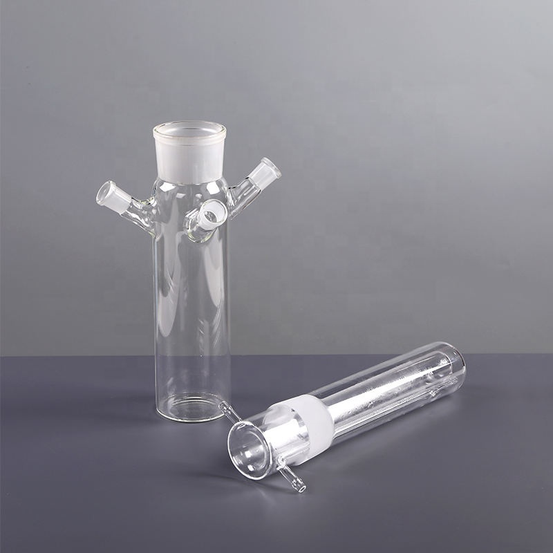
Customized High-Purity Quartz Glass Reactor Container
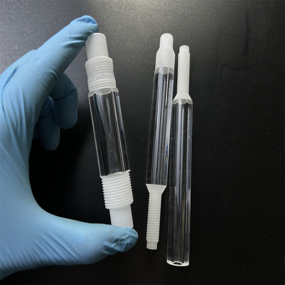
Customized High Purity Threaded Transparent UV Quartz Glass Tube
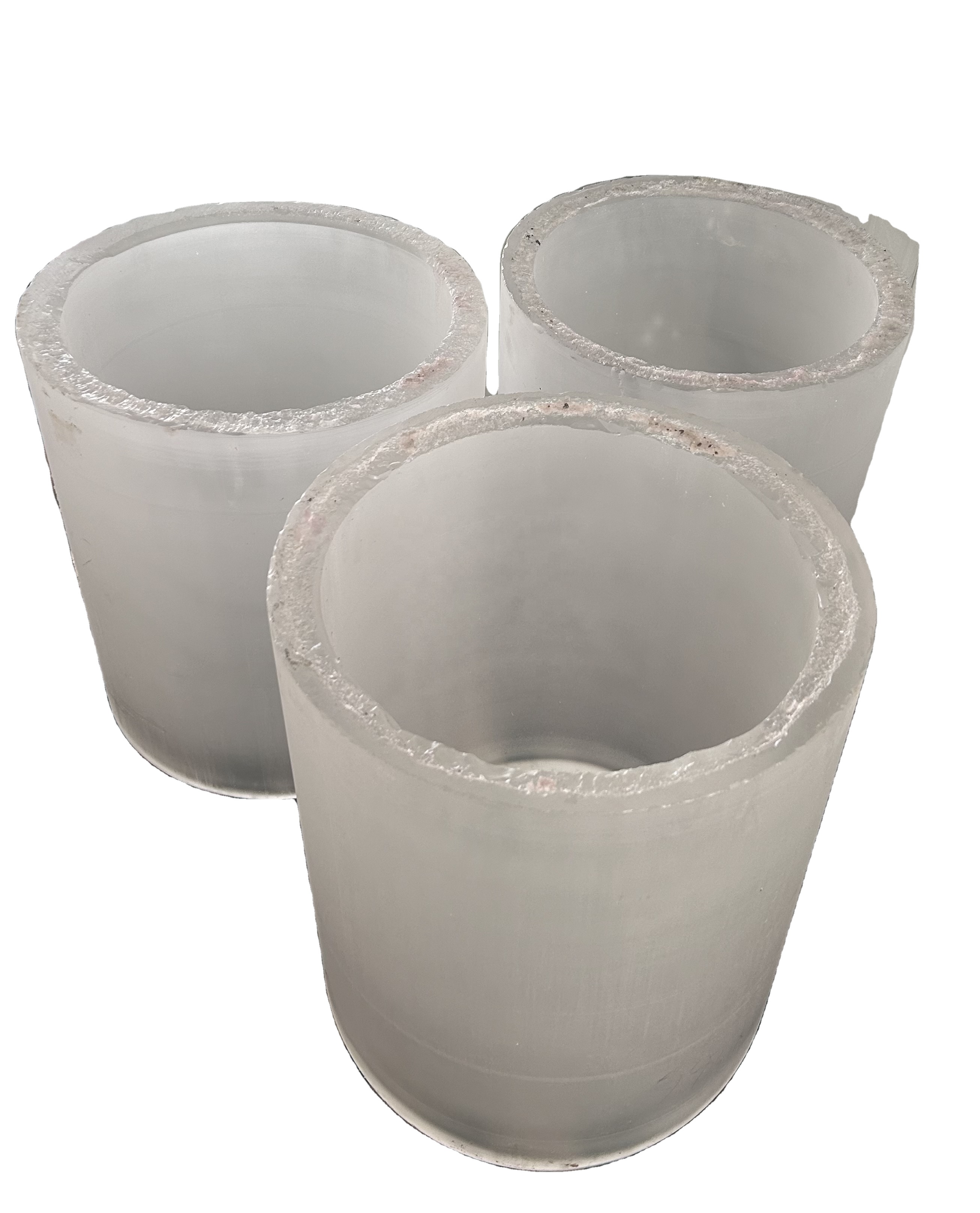
Open Ended Fused Quartz Frosted Glass Cylinder Ingot
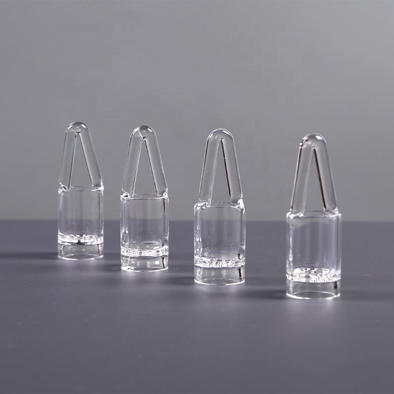
Factory Custom High Pressure 99.99% Pure Quartz Glass Tube
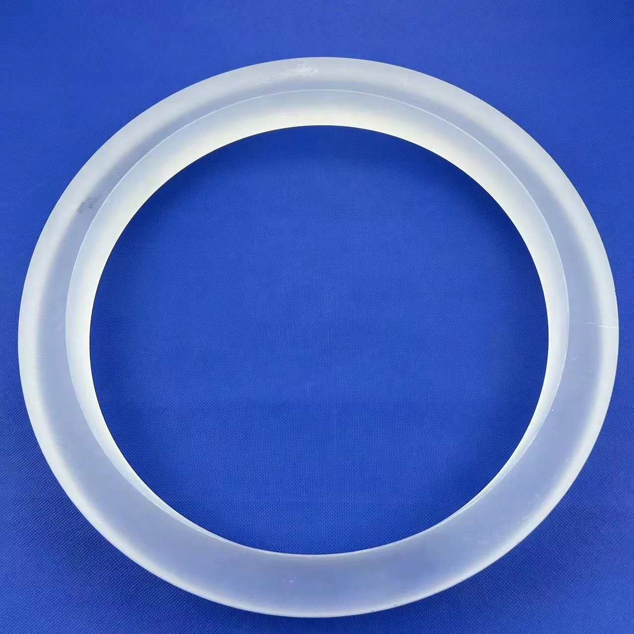
Custom Coated 99.99% Pure Quartz Rings for Semiconductor CVD
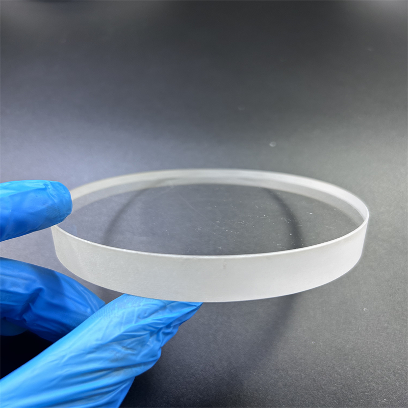
High Temperature Transparent UV Quartz Glass Plate Polished
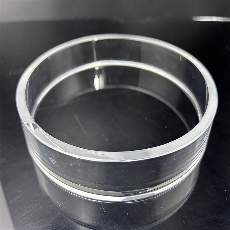
High Transparent Corrosion-Resistant Fused Quartz Bell Jar
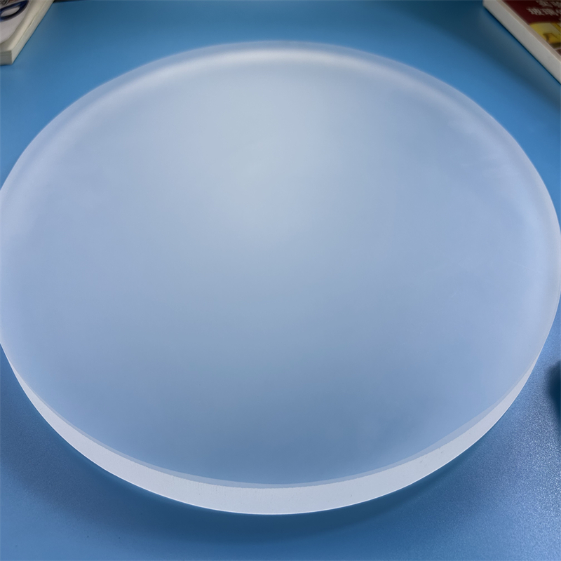
High Temperature Resistance Frosted Quartz Disc / Plate
Critical Role of Fused Quartz Rings in 200mm/300mm Semiconductor Fab Yields
In cutting-edge sub-7nm dry etch (RIE, ICP, CCP), chemical vapor deposition (LPCVD, PECVD, ALD), and rapid thermal processing (RTP) chambers, semiconductor quartz rings serve as critical structural consumables. Operating directly adjacent to the silicon wafer edge, quartz focus rings, retaining rings, and dielectric shield rings control the RF electrical sheath, maintain plasma density uniformity across wafer peripheries, and safeguard underlying electrostatic chucks (ESC) against reactive halogen plasma attack.
Even trace metallic contamination at the parts-per-billion (ppb) level can cause fatal gate oxide breakdown, carrier lifetime deterioration, or localized parasitic capacitance in modern 3D NAND and FinFET/GAAFET architectures. Lianyungang Zelvo Quartz Products Co., Ltd., based in Donghai—the world-renowned hub of China's quartz reserves—synthesizes and fabricates optical and electric-arc fused quartz with stringent control over trace transition metals (Fe ≤ 0.2 ppm, Cu ≤ 0.05 ppm, Ni ≤ 0.05 ppm) and mobile alkali elements (Na, K, Li ≤ 0.5 ppm).
ICP-MS Trace Impurity Profiling: Industry Standards vs. Zelvo Ultra-Purity Quartz
The table below details typical glow discharge mass spectrometry (GDMS) and inductively coupled plasma mass spectrometry (ICP-MS) impurity benchmarks for semiconductor fab-grade quartz rings:
| Chemical Element | Symbol | Commercial Grade (ppm) | Semiconductor Standard (ppm) | Zelvo Fab-Grade Ultra Quartz (ppm) | Detection Method |
|---|---|---|---|---|---|
| Aluminum | Al | 14.0 – 20.0 | ≤ 8.00 | 3.20 – 5.50 | ICP-MS Passed |
| Iron | Fe | 0.80 – 1.50 | ≤ 0.30 | 0.08 – 0.15 | ICP-MS Passed |
| Sodium | Na | 1.00 – 2.00 | ≤ 0.50 | 0.12 – 0.28 | AAS / ICP-MS |
| Potassium | K | 1.00 – 1.80 | ≤ 0.40 | 0.10 – 0.25 | AAS / ICP-MS |
| Lithium | Li | 0.50 – 1.00 | ≤ 0.20 | 0.03 – 0.08 | ICP-MS Passed |
| Calcium | Ca | 1.00 – 2.50 | ≤ 0.60 | 0.20 – 0.45 | ICP-MS Passed |
| Copper | Cu | 0.05 – 0.10 | ≤ 0.02 | < 0.005 (Undetectable) | High-Res ICP-MS |
| Hydroxyl Group (OH⁻) | OH | 150 – 250 | ≤ 30 (Dry Etch) / ≤ 5 (Low OH) | < 15 (Electrically Fused) | FTIR Spectroscopy |
Note: Lower OH⁻ (Hydroxyl) content is strictly maintained for high-temperature diffusion and etch ring applications to prevent high-temperature structural devitrification (cristobalite formation) and minimize RF power dissipation during wafer processing.
Why Global Tier-1 Wafer Fabs Source from Zelvo Quartz
Located in Donghai County, China's Silicon & Crystal Capital, Lianyungang Zelvo Quartz Products Co., Ltd. combines sovereign natural quartz supply chain integration with high-precision CNC machining lines.
Onsite-Verified Fab
Audited premises with complete tracing from quartz sand smelting, ingot thermal annealing, to class 1,000 cleanroom ultrasonic packing.
≤ 2-Hour Response
Engineers directly evaluate 2D CAD/3D STEP drawings. Comprehensive quotation, tolerance feasibility analysis, and lead times provided without delay.
High Reorder Rate (37%)
Trusted across North America, Southeast Asia, and Europe. Our 4.9/5 buyer satisfaction reflects zero-defect dimensional and packaging reliability.
Safe Clean-Fab Export
RCA cleanroom chemical stripping, vacuum double-poly bagging, and custom shock-absorbing foam wooden crates preventing edge chipping.
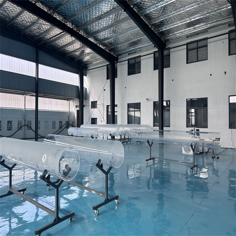
Precision CNC Machining Center
5-Axis ultrasonic milling machines carving focus rings to ±0.005mm.

Thermal Annealing & Flame Polishing
1215°C stress-relief annealing preventing micro-fractures under RF thermal shocks.
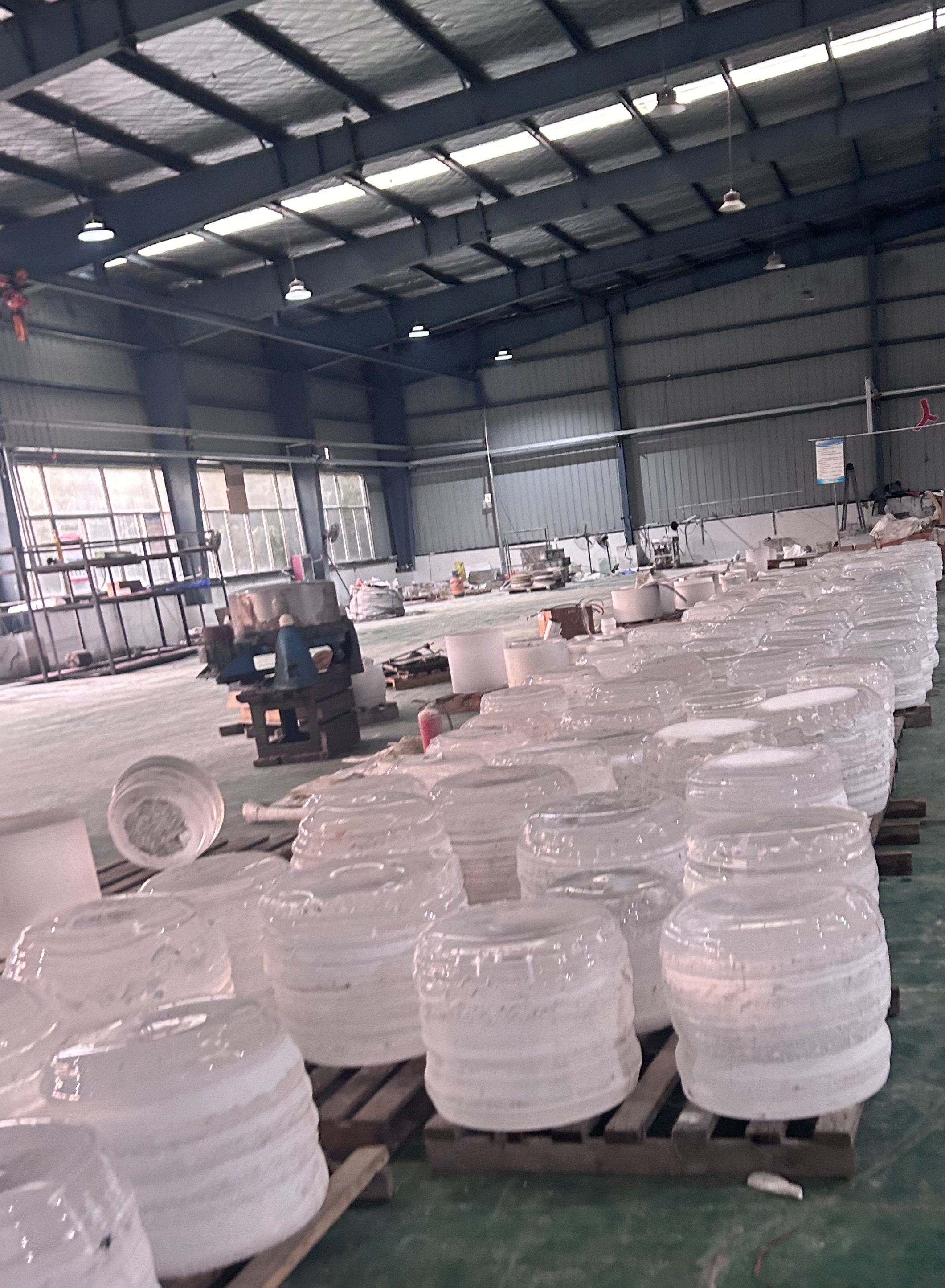
Polariscopic & CMM Metrology
100% laser interferometry, surface roughness (Ra), and internal stress testing.
Global Procurement Trends in Semiconductor Quartz Consumables
As the semiconductor equipment consumables market exceeds US$8.4 Billion, wafer fabricators and fab managers face critical shifts driven by sub-2nm gate geometries, high-aspect-ratio (HAR) contact etch depths, and global fab capacity expansion across the Americas, Europe, and Asia. Fab procurement heads must navigate four crucial sourcing dynamics:
1. Transition to Synthetic Fused Silica
While electrically fused natural quartz remains cost-efficient for furnace liners, advanced plasma etch rings require synthetic silica with parts-per-trillion (ppt) purity and micro-bubble class 0 ratings to mitigate micro-trenching.
2. Dual-Sourcing & OEM Equivalency
Fabs are actively breaking single-source dependency on tool OEMs (Applied Materials, Lam Research, Tokyo Electron). Precision non-OEM second-source manufacturers offering 100% drawing compliance are securing long-term blanket purchase agreements (BPAs).
3. Erosion-Resistant Coating Tech
Increasing plasma bias voltages accelerate quartz ring consumption. The procurement market is shifting toward specialty yttrium oxide (Y₂O₃) and fluoride-doped quartz coatings to extend mean time between cleans (MTBC) from 250 RF hours to over 700 RF hours.
4. Strict Digital CoC & FAIR Audits
Procurement contracts increasingly require Digital First Article Inspection Reports (FAIR), laser surface profiling certificates, full raw-material lot traceability, and residual stress birefringence maps prior to customs clearance.
Technological Trends: Overcoming Plasma Erosion & Particulate Shedding
As wafer fabrication advances into high-density 3D stacking (3D NAND architectures surpassing 300 active layers), dielectric dry etching relies on extremely aggressive fluorocarbon plasma chemistries (C₄F₈, C₄F₆, CH₂F₂) combined with high RF bias voltages exceeding 5,000 W. Under these extreme conditions, standard quartz components face physical ion bombardment sputtering and chemical volatilization (forming SiF₄ gas):
Chemical Plasma Reaction: SiO₂ (s) + 4F* (plasma) → SiF₄ ↑ (g) + O₂ / O* (g)
When natural quartz with micro-porosities or subsurface micro-fractures is exposed to this plasma, differential etch rates along crystalline grain boundaries cause catastrophic particulate shedding onto silicon wafers. Zelvo Quartz mitigates this failure mode through advanced production protocols:
- Subsurface Damage Elimination: Utilizing multi-stage diamond grinding (from coarse D120 to ultra-fine D800 resin-bonded diamond abrasives) followed by chemical-mechanical chemo-polishing (CMP) to achieve sub-nanometer surface roughness (Ra ≤ 0.2 µm) and eradicate micro-cracking.
- Thermal Stress Homogenization: Stepwise computer-controlled thermal annealing cycles holding parts at 1150°C – 1215°C, followed by a controlled 1.5°C/min slow ramp down through the strain point (1070°C) to eliminate residual birefringence (≤ 10 nm/cm).
- Laser Non-Contact Trepanning: High-energy CO₂ and femtosecond laser drilling and edge trepanning to avoid micro-chipping on delicate wafer alignment pins and gas showerhead holes.
Semiconductor Quartz Procurement FAQ
Direct technical answers addressing purity validation, dimensional tolerances, plasma etch lifetimes, and clean packaging standards.
What is the purity standard of your semiconductor-grade fused quartz rings?
Can you fabricate custom quartz focus rings and chamber components directly from CAD drawings?
What are the maximum operational temperatures and thermal shock limits for your quartz parts?
How do you manage cleanroom packaging and avoid particulate contamination during transit?
What is your Minimum Order Quantity (MOQ) and production turnaround for prototypes?
What international trade terms and payment methods do you support?
Accelerate Your Fab Sourcing with China's Premier Quartz Exporter
Submit your CAD drawing, technical specifications, or OEM replacement part number today. Our senior semiconductor materials engineering team will review manufacturability, verify tolerances, and deliver an actionable technical quote within 2 hours.