High-Purity Fused Quartz & Silica Engineered Components
Certified 99.999% SiO₂ fused silica substrates, CVD rings, vacuum reaction tubes, and laser-machined wafer optics engineered for ultra-high temperature resistance, deep ultraviolet (DUV) transmission, and aggressive plasma durability.
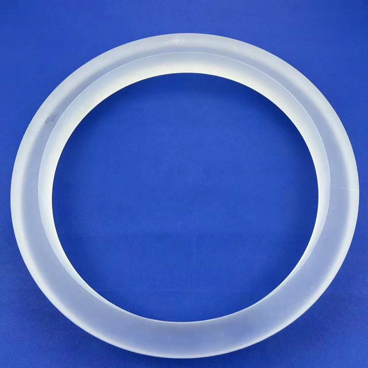
Custom Coated 99.99% Pure Quartz Rings for Semiconductor CVD Optics
Designed for etch-resistant dry chemical vapor deposition (CVD) tools and optical clamping rings with micro-machined thermal grooving.
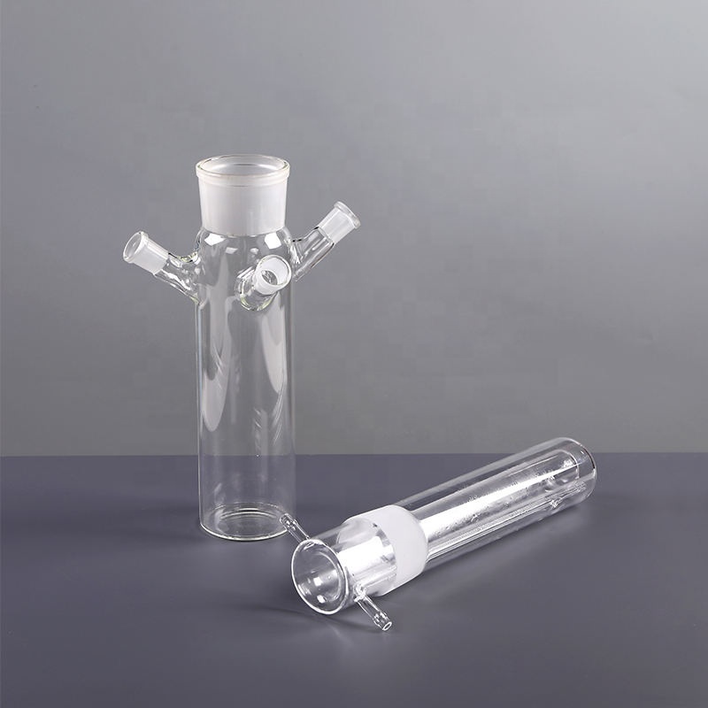
Customized High-Purity Quartz Glass Reactor Container
Precision-blown quartz reactor vessels with high UV transmission chambers for photochemical degradation and wet chemical synthesis.
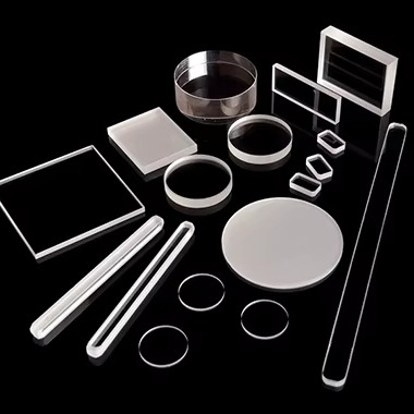
Custom High-Temperature Fused Transparent Quartz Optical Test Sheet
Double-side planetary polished optical inspection substrates for laser windows, XRD sample slide arrays, and aerospace sensor covers.
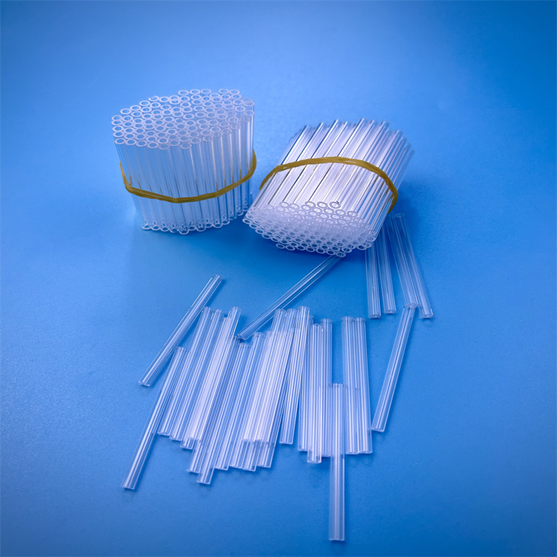
High Quality Transparent U-Bent Quartz Glass Tube Bending Service
Precision multi-axis hot-forming tube lines for ultraviolet germicidal systems, high-temperature fluidic loops, and heat exchange manifolds.
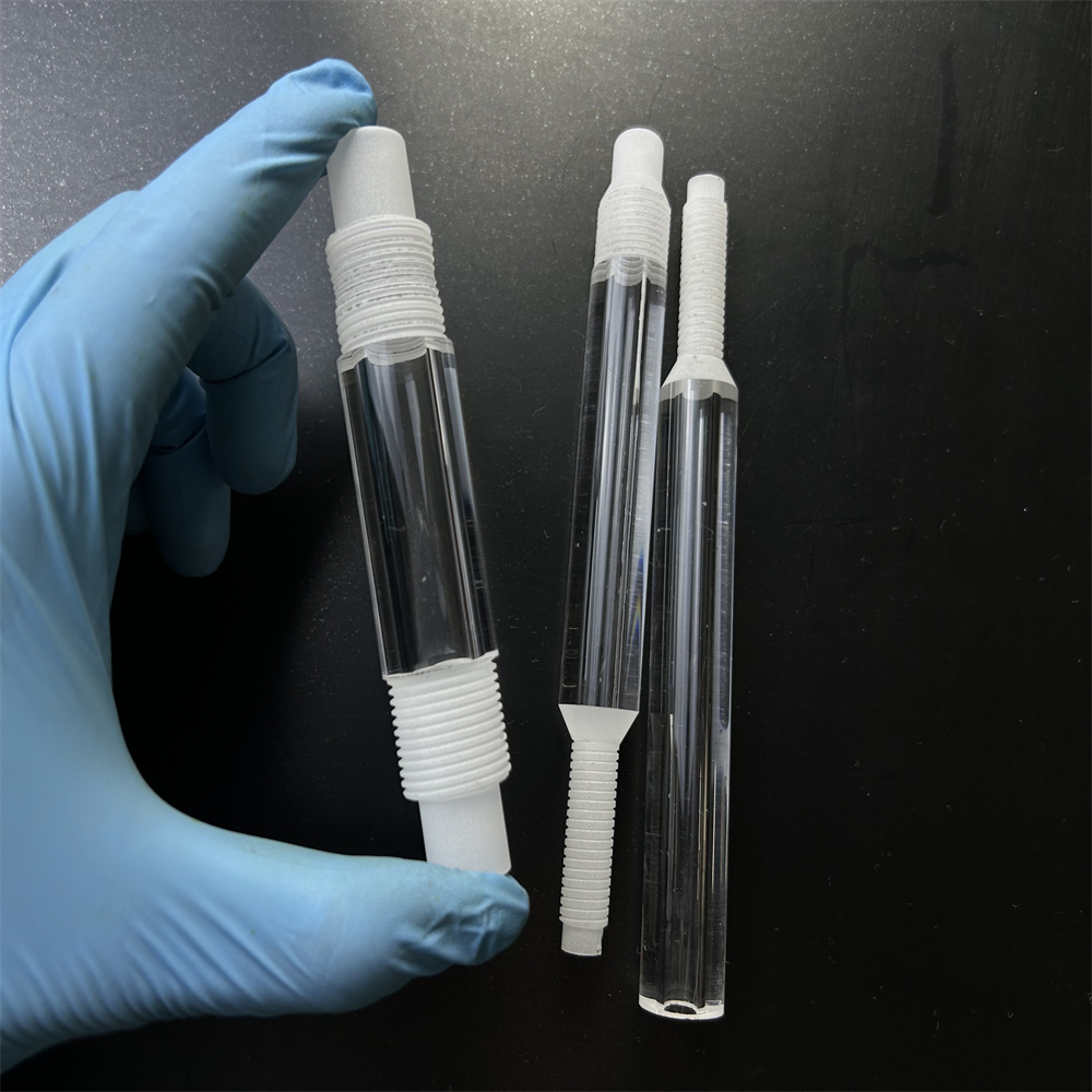
Custom High Purity Threaded UV Quartz Glass Tube
Engineered threaded interface tubes delivering mechanical seal integrity under high vacuum and deep UV lithography illumination pipelines.
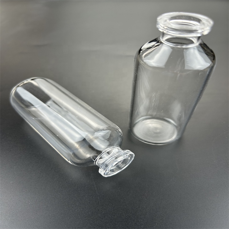
Medical-Grade Corrosion-Resistant Ozone-Free Quartz Ampoules
Ultra-pure quartz ampoules for pharmaceutical standard storage, high-pressure cryo-preservation, and corrosive reagent micro-containment.
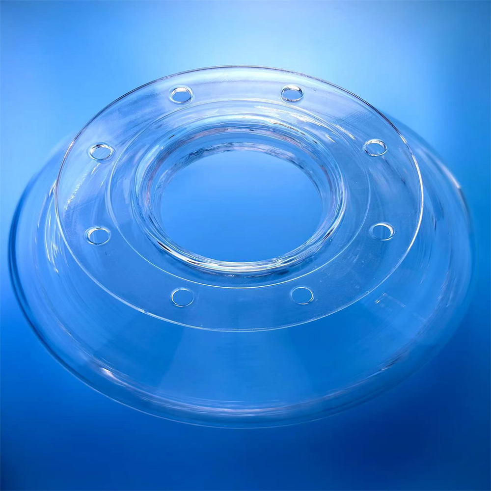
Custom Thickness Twin-Tube Clear High-Purity Flanged Quartz Tube
Twin-channel fused silica conduits featuring custom ground flat-faced flanges for vacuum furnace monitoring and dual pyrometry probes.
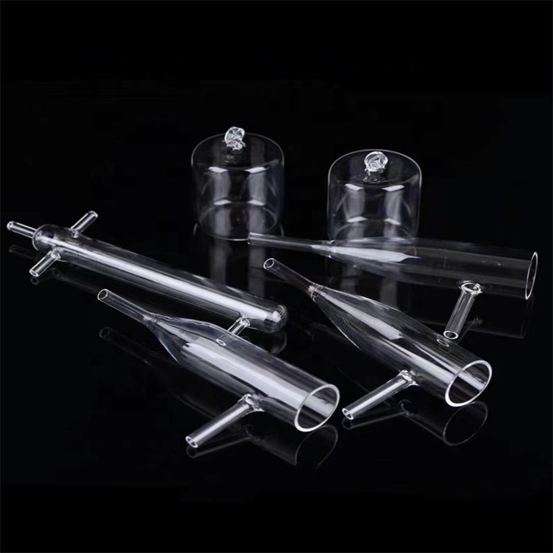
Laboratory High-Temperature Twin Tube Quartz Glass for CVD Furnaces
Heavy-wall dual furnace tubes designed for thermal shock resistance in extreme vacuum diffusion furnaces, ALD rigs, and graphene synthesis.
Engineering Whitepaper: Synthetic Fused Silica vs. Natural Fused Quartz
Precision selection criteria for design engineers across the Southern California aerospace corridor and optical research laboratories.
| Physical / Optical Property | JGS1 (UV Synthetic) | JGS2 (Optical Quartz) | JGS3 (IR Fused Quartz) |
|---|---|---|---|
| Transmission Bandwidth | 185 nm – 2500 nm | 220 nm – 2500 nm | 260 nm – 3500 nm |
| SiO₂ Purity Level | ≥ 99.9999% | ≥ 99.99% | ≥ 99.99% |
| Hydroxyl [OH⁻] Content | < 1000 – 1200 ppm | < 150 – 200 ppm | < 5 – 8 ppm (Water-free) |
| Coefficient of Thermal Expansion | 5.5 × 10⁻⁷ / K | 5.5 × 10⁻⁷ / K | 5.4 × 10⁻⁷ / K |
| Surface Flatness Capability | λ/10 @ 632.8 nm | λ/4 @ 632.8 nm | λ/4 @ 632.8 nm |
| Surface Roughness (Ra) | < 0.3 nm (Super-polish) | < 0.5 nm | < 0.8 nm |
| Laser Damage Threshold (LIDT) | > 25 J/cm² (1064nm, 10ns) | > 12 J/cm² | > 10 J/cm² |
| Continuous Strain Point | 1070 °C | 1120 °C | 1125 °C |
| Softening Point | 1683 °C | 1683 °C | 1680 °C |
Sub-Nanometer Deterministic Finishing for Extreme Environments
Fused silica ($SiO_2$) represents the pinnacle of optical glass performance due to its amorphous, non-crystalline tetrahedral microstructure. In contrast to borosilicate or crown glass, fused silica delivers an extraordinarily near-zero thermal expansion coefficient ($5.5 \times 10^{-7}/\text{K}$ between 20°C and 320°C), making it the single most reliable material for spaceborne optics, high-energy laser mirrors, and lithography mask blanks where thermal deflection cannot exceed fractions of an optical fringe.
Custom OEM/ODM Polishing & CNC Ultrasonic Machining
We leverage multi-axis ultrasonic core drilling, 5-axis CNC radius profiling, and double-sided pitch lapping to fabricate complex geometric features down to ±0.005 mm mechanical tolerances, with laser damage threshold (LIDT) capabilities exceeding 20 J/cm² for Nd:YAG harmonic applications.
Our manufacturing line integrates 100% spectrophotometer spectral verification from deep ultraviolet (DUV 193nm) to short-wave infrared (SWIR 2500nm). With bubble inclusions controlled to Class 0/DIN 3140 and wavefront distortion below $\lambda/10$, our substrates ensure near-zero wavefront aberration under extreme mechanical stress.
Los Angeles & Southern California Application Scenarios
How our fused silica substrates and quartz glass hardware empower the leading aerospace, defense, semiconductor, and biotechnology enterprises across the Southland.
Aerospace & Commercial Space Flight
Operating directly with defense primes and private orbital space exploration firms concentrated in El Segundo, Hawthorne, and Long Beach. Our UV-grade fused silica substrates serve as optical sensor observation windows, retroreflectors, and star tracker viewport blanks subjected to orbital vacuum and rapid thermal cyclings between -150°C and +150°C.
Directed Energy & High-Energy Lasers
Supplying high laser-damage threshold (LIDT) synthetic fused silica beam splitter substrates and laser debris shields for defense photonics research centers along the Point Mugu and China Lake naval test corridors. Engineered with internal stress birefringence below 5 nm/cm to prevent thermal lensing under multikilowatt continuous wave (CW) excitation.
Quantum Optics & Pasadena Photonics Hub
Partnering with advanced research institutions and quantum technology startups across Pasadena and Silicon Beach. Providing ultra-pure JGS1 synthetic silica micro-cavity resonators, vacuum viewports, and non-fluorescent optical flats for cold-atom magneto-optical traps (MOT) requiring exceptional optical surface micro-roughness (Ra < 0.3 nm).
Sub-Micron Semiconductor & MEMS Fabs
Supporting wafer processing lines and foundry pilot labs throughout Southern California and Irvine. Our OEM quartz ware includes 200mm/300mm diffusion boat carriers, plasma-enhanced atomic layer deposition (ALD) injector tubes, and high-purity single-crystal substrate holders engineered to prevent heavy metal contamination during thermal anneals.
Biophotonics & Microfluidics Diagnostics
Engineered for Thousand Oaks and San Diego biotech research parks. Custom laser-cut fused silica flow cell plates and UV fluorescence windows offering negligible auto-fluorescence, absolute chemical inertness to enzymatic buffers, and precision micromachined fluidic channels down to 50-micron track widths.
Thermal Analysis & XRD Spectroscopy
Delivering low-background slotted XRD sample holders, BET adsorption sample tubes, and twin-bore pyrometry shields to commercial metallurgical testing laboratories and university materials departments across Greater Los Angeles. Zero crystalline phase inversion up to 1100°C continuous operational stress.
Los Angeles Market Trends: Fused Silica Substrates (2025–2030)
Deep-tech manufacturing in Southern California is undergoing rapid transformation, propelled by aerospace modernization, domestic semiconductor resilience, and advanced laser platforms.
SmallSat & Satellite Mega-Constellations
With Los Angeles remaining the premier global capital for commercial space transport, the demand for lightweight, radiation-hardened fused silica optical solar reflectors (OSR) and optical communication transceivers has surged. Substrates must maintain high UV transparency without solarization darkening across multi-year low Earth orbit (LEO) radiation missions.
Extreme Ultraviolet (EUV) & DUV Lithography Testing
Local semiconductor design validation and advanced packaging facilities require fused silica mask substrates with ultra-stringent surface micro-roughness below 0.3 nm RMS. Synthetic JGS1 formulations with near-zero hydroxyl (OH) content ensure minimal phase deformation in advanced 3nm and below exploratory lithographic processes.
Supply Chain Reshoring & Express Port Clearance
California buyers are demanding diversified sourcing combining scalable offshore manufacturing cost-efficiencies with transparent customs clearance into the Port of Los Angeles (POLA) and express air consolidation at LAX. Traceability documentation, full material test reports (MTR), and rapid-turn prototype sampling are paramount.
Global Manufacturing Scale Combined with Local Engineering Support
Headquartered in Donghai—the world's capital of natural and synthetic quartz refining—we supply tier-one OEMs, research institutes, and defense contractors across North America with certified optical components.
99.999% Raw Material Purity
Direct mine-to-furnace integration in Donghai ensuring complete elimination of alkali contaminants and minimal trace heavy elements (Fe < 0.2 ppm, Al < 8 ppm).
≤ 2-Hour Response Time
Dedicated English-speaking technical account managers and optical engineers provide rapid drawing reviews, CAD/CAM verification, and comprehensive DFM analysis.
Flexible MOQ Starting at 1 Piece
We eliminate high minimum run barriers for R&D laboratories, university cleanrooms, and engineering prototyping while retaining high-volume multi-thousand piece automated scale.
Zero-Damage Export Crating
Custom multi-layer shock absorbing polyethylene foam lining, desiccated vacuum packaging, and ISPM-15 certified wooden cases engineered for trans-Pacific and express air logistics.
Frequently Asked Questions: Sourcing Fused Silica in Los Angeles
Essential engineering and procurement answers covering optical specifications, thermal limits, ITAR considerations, and international logistics.
What is the difference between synthetic fused silica (JGS1) and fused quartz (JGS2/JGS3) when specifying optical substrates?
How does your factory ensure compliance with US commercial and aerospace procurement standards?
What are the standard delivery lead times and customs logistics procedures for shipments to Los Angeles?
Can you provide custom anti-reflective (AR) and dielectric coatings on fused silica substrates?
What is your maximum machining size capacity for custom quartz plates and heavy-wall tubes?
How does fused silica perform under extreme thermal cycling and rapid liquid nitrogen quenching?
Submit Your Custom Quartz Drawing for Rapid Engineering Review
Whether you require a single high-precision prototype for an experimental aerospace testbed in El Segundo, or continuous container-load delivery of furnace tubes for commercial semiconductor manufacturing, our engineering group will assess your dimensional tolerances and return a formal DFM review within 2 working hours.