High-Performance Fused Quartz Products & Custom Fabrication
Direct from our manufacturing workshop: certified fused quartz glass plates, multi-bore reaction tubes, and CNC-machined CVD apparatus engineered to withstand severe thermal, chemical, and vacuum environments.
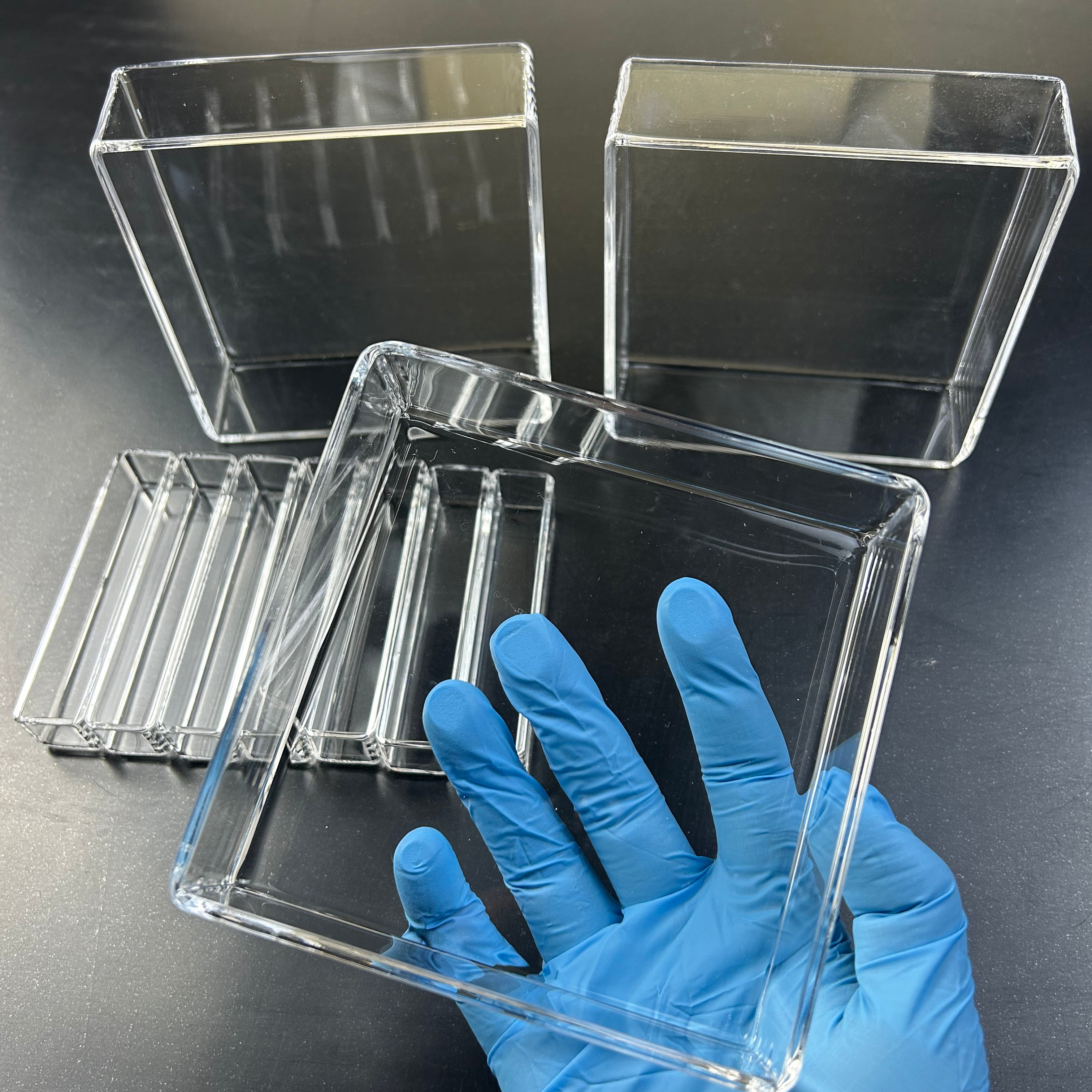
Customized Fused Quartz Cylinder Crucible & Process Tank
- Purity Rating: ≥ 99.99% Fused SiO₂
- Thermal Limit: 1100°C Cont. / 1300°C Peak
- Fabrication: Flame Welded & Annealed
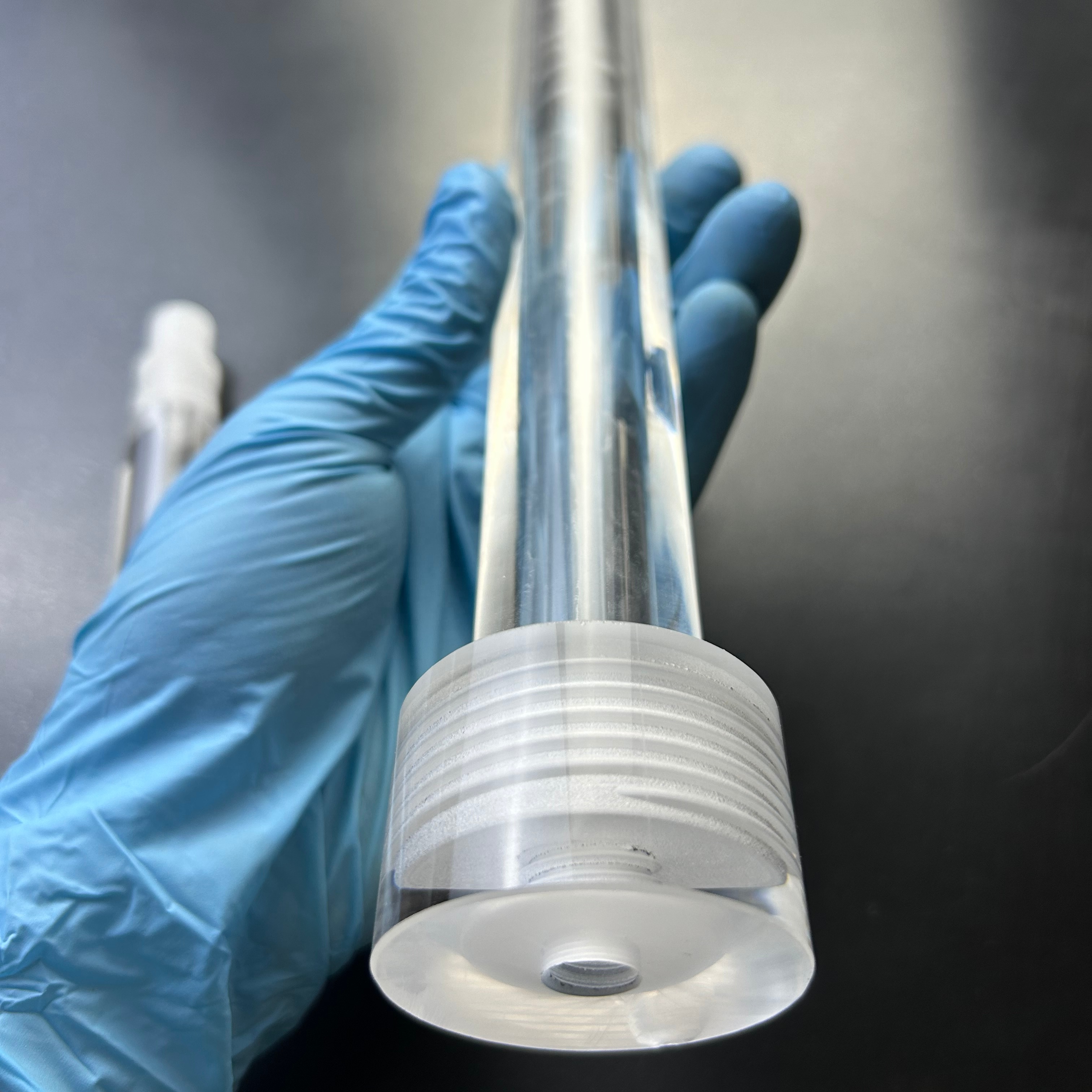
High-Pressure Polished Quartz Glass Twin Tube
- Configuration: Twin-Bore Precision Parallel
- Surface Finish: Fire Polished & Optical Clear
- Processing: Bending / CNC Cutting
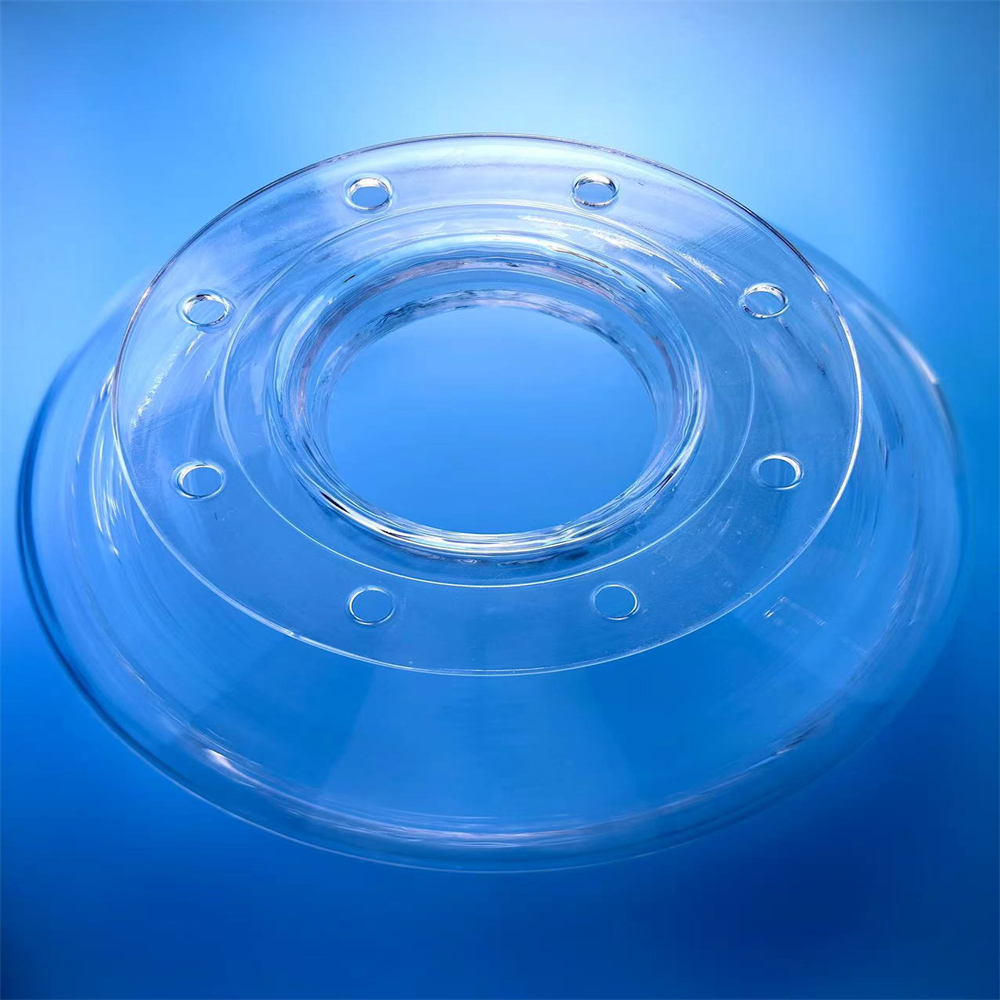
Flanged Twin Quartz Tube & Polished Flange Ring
- Connection: Ground Joint / Polished Flange
- Tolerance: ±0.05 mm on Flange Face
- Application: Vacuum CVD & Epi Reactors
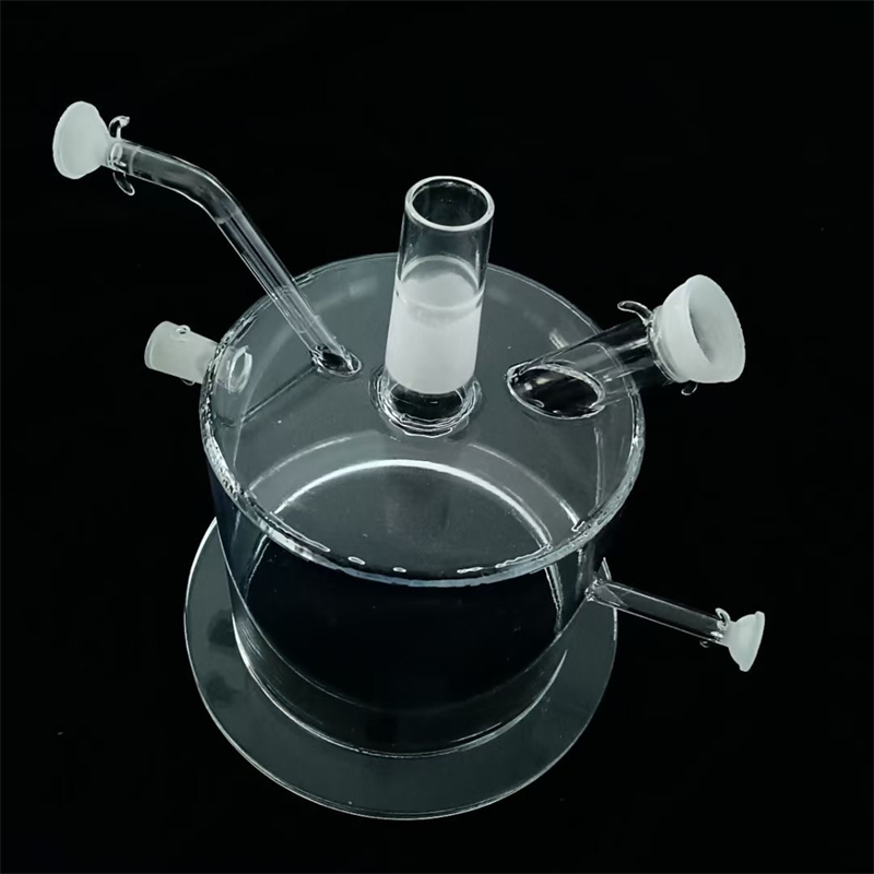
Ozone-Free High-Pressure Clear Quartz Process Tube
- Optical Grade: Ozone-Free UV/IR Polished
- Pressure Resistance: Custom Heavy-Wall Build
- Processing: Rotary Cutting & Flame Glazing
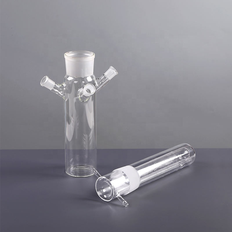
Photocatalytic Internal Illumination Quartz Reactor
- Spectral Band: High Deep-UV Transmission
- Design: Internal Jacket & Cooling Well
- Application: Photochemical Synthesis
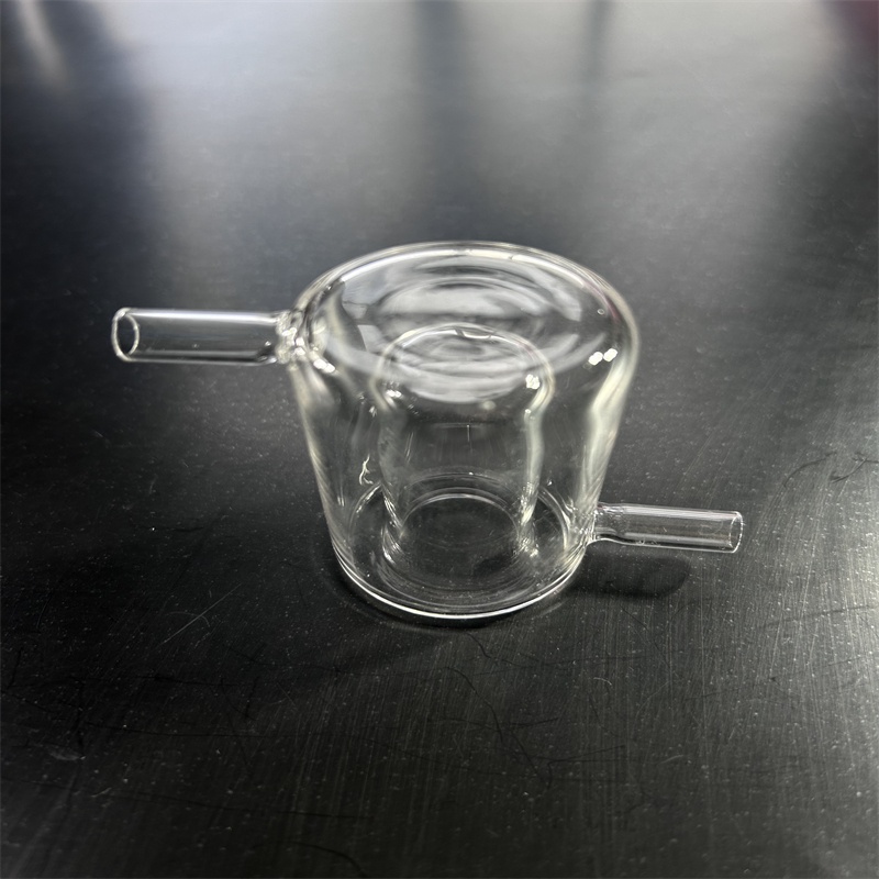
Laboratory Twin-Tube Quartz Reaction Vessel
- Joining: Seamless Optical Hydrogen Flame
- Corrosion Rate: Zero in Acidic Medium (excl. HF)
- Service: Drawing-Based Lab Apparatus
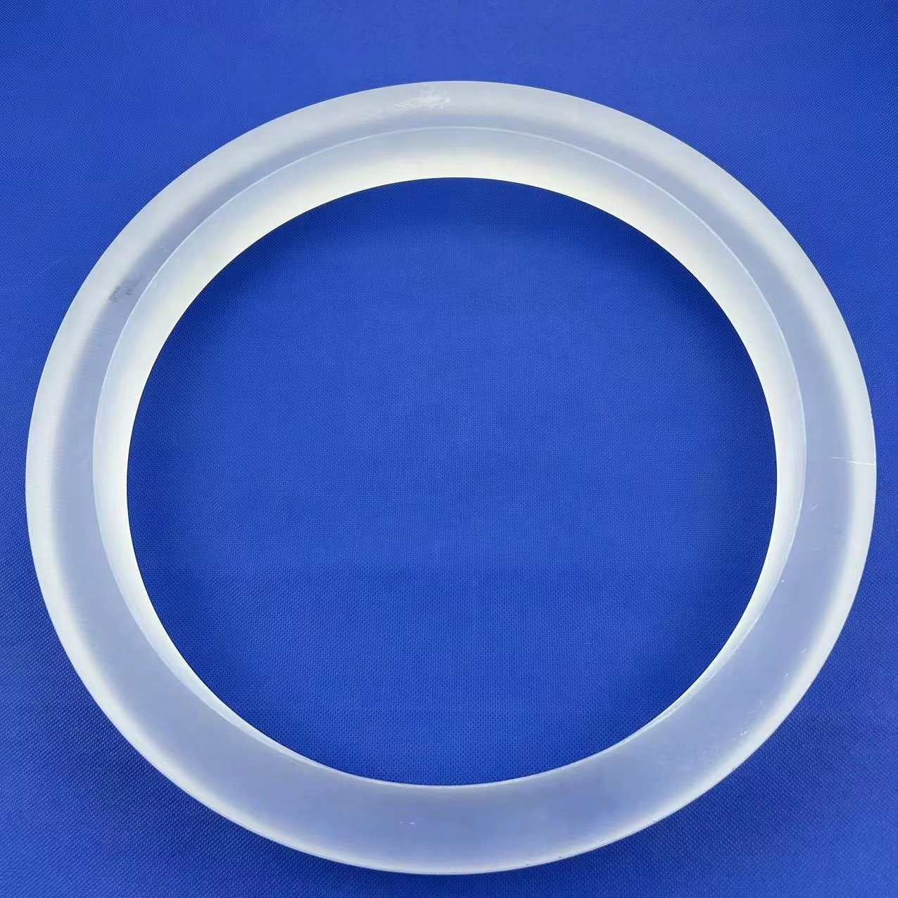
High-Purity Coated Quartz Rings for Semiconductor CVD
- Tolerance: CNC Machined to ±0.02 mm
- Surface: Optical Lapped / Custom Coated
- Application: Etch Rings & Plasma Shields
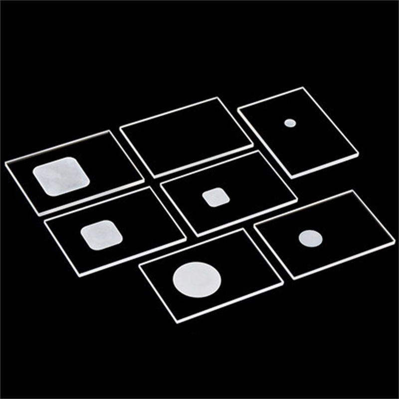
Slotted Fused Quartz Sheet & XRD Sample Carrier
- Machining: Laser Micro-Grooving & Dicing
- Background: Zero Amorphous XRD Scattering
- Flatness: λ/4 per 25mm Wavefront
Engineering Dominance: The Donghai Industrial Quartz Cluster
Lianyungang Zelvo Quartz Products Co., Ltd. operates at the core of Donghai County, Jiangsu Province—globally acknowledged as China's silica capital. Combining direct access to the world's most concentrated high-purity natural silica reserves with over a decade of precision glass-blowing, CNC milling, and laser drilling, we bridge the gap between raw silica ingot processing and cleanroom-ready semiconductor components.
99.99% SiO₂ Purity Control
Our raw quartz ingots undergo hydrofluoric/nitric acid pickling, electrostatic separation, and vacuum electro-fusion. Total metallic impurities (Fe, Al, Ca, Mg, Ti, Na, K, Li) remain consistently under 15–20 ppm, ensuring zero dopant outgassing in high-temperature semiconductor furnaces.
Sub-Micron CNC & Laser Micro-Machining
Equipped with 5-axis ultrasonic CNC grinding centers, high-speed diamond wafer saws, and pulsed fiber laser drilling stations. We fabricate slotted sample holders, microfluidic quartz plates, and beveled wafer rings down to ±0.01 mm dimensional tolerances without micro-fractures.
Onsite-Verified & Rapid DFM Engineering
Our full facility and corporate registration are legally audited and onsite-checked by third-party inspectors. We operate an agile engineering bureau providing comprehensive Design For Manufacturability (DFM) reviews and formal quotes within 2 hours of drawing receipt.
1-Piece Prototyping to High-Volume Runs
Unlike state-run raw material conglomerates that require multi-ton minimums, we nurture research labs and specialized industrial equipment builders with an absolute 1-piece MOQ for bespoke drawings, backed by multi-layered cleanroom vacuum packaging and worldwide air freight.
Thermal, Optical & Mechanical Performance Benchmarks
When procuring precision quartz plates and windows, design engineers must distinguish between Electrically Fused Natural Quartz (Type II) and Synthetic Chemical Vapor Deposition Fused Silica (Type III / JGS1). Fused quartz is engineered through the continuous electric resistance melting of high-purity natural silica sand under inert atmosphere, maximizing refractory resistance up to 1300°C with an ultra-low hydroxyl (OH) content (< 5 ppm).
Synthetic fused silica, produced by hydrolyzing volatile silicon tetrachloride (SiCl₄) in an oxy-hydrogen flame, features near-zero trace metals (< 0.1 ppm) and exceptional deep-ultraviolet (DUV) transparency down to 185 nm, making it indispensable for excimer laser optics, semiconductor photolithography, and UV-curing windows.
Both material variants exhibit an exceptionally low coefficient of thermal expansion (α = 5.5 × 10⁻⁷ /°C) between 20°C and 320°C. This allows a 10mm thick quartz plate to be heated red-hot to 1100°C and plunged directly into ice water at 0°C without catastrophic mechanical cracking or structural stress delamination.
| Physical Property (20°C) | Standard Value | Engineering Significance |
|---|---|---|
| Chemical Purity (SiO₂) | ≥ 99.992% | Guarantees zero furnace contamination |
| Density (ρ) | 2.20 ± 0.02 g/cm³ | Ultra-compact non-porous structure |
| Thermal Expansion (α) | 5.5 × 10⁻⁷ /°C | Zero thermal shock rupture up to 1100°C |
| Softening Point | 1683°C | Exceeds extreme refractory thresholds |
| Annealing Point | 1215°C | Residual thermal stress relief baseline |
| Strain Point | 1120°C | Continuous structural load-bearing limit |
| Dielectric Strength (1 MHz) | 5.0 × 10⁷ V/m | Premium RF/Microwave transparent insulator |
| Refractive Index (n_d) | 1.4585 | Low optical dispersion across spectra |
| Mohs Hardness | 5.5 – 6.5 | High scratch resistance and wear life |
Future Sourcing & Technology Trends in Quartz Components
The global high-purity quartz glass plate and component sector is undergoing a rapid transition triggered by high-density semiconductor fabrication, next-generation solar cells, and harsh-environment photonic systems.
Plasma-Resistant CVD & Etch Component Evolution
As semiconductor wafer fabrication migrates beneath the 3nm threshold and 3D-NAND architectures stack past 300 layers, fluorine and chlorine-based plasma etch chambers demand quartz plates and rings with significantly enhanced surface integrity. The industry is rapidly adopting high-density flame-polished and doped fused silica with near-zero bubble density (DIN 58927 Class 0) to prevent micro-particle spalling that degrades wafer yield.
Large-Format Thin Plates for TOPCon & Perovskite
With TOPCon and tandem Perovskite-Silicon PV cells displacing legacy PERC production, thermal diffusion and atomic layer deposition (ALD) stages require large-aperture quartz plates exceeding 1200mm × 800mm with wall thickness uniformity of ±0.05 mm. Buyers are securing guaranteed long-term allocations from verified Chinese exporters that integrate electric fusion ingots directly into high-precision CNC slicing operations.
Direct-From-Cluster Turnkey Machining Over Raw Stock
Global optical and lab equipment OEMs are abandoning the two-tier procurement model—purchasing rough quartz blanks in Asia and shipping them to Western optical shops for milling. Instead, buyers are selecting turnkey precision suppliers in Donghai, Jiangsu, who execute laser core-drilling, surface chemical mechanical polishing (CMP to Ra < 0.5nm), and spectrophotometric validation before export, cutting supply chain lead times by 60%.
Strict Inspection Protocol for Exported Quartz Plates
Every batch of fused quartz plates and custom glass instruments leaving our Lianyungang manufacturing plant follows a rigorous 4-stage metrological verification sequence, documented with material certificates and optical test sheets.
Raw Material ICP-OES Traceability
Raw silica ingots undergo Inductively Coupled Plasma Optical Emission Spectrometry to test for metallic trace cations (Al, Fe, Ti, Ca, Mg, Na, K, Li). Only ingots certified at ≥ 99.99% SiO₂ are approved for semiconductor wafer plate slicing.
Dimensional & Interferometric Sizing
Plates and machined slotted carriers are inspected using coordinate measuring machines (CMM) and laser micrometer gauges. Planar optical windows are checked on a Zygo laser interferometer to verify flatness within λ/4 to λ/10 per inch.
Stress Birefringence Polariscope Scan
All fire-bent and welded quartz reactors undergo automated polariscope examination to assess residual stress. If photoelastic retardation exceeds 10 nm/cm, components undergo secondary computerized annealing at 1215°C.
Cleanroom Vacuum Packing & Crate Logistics
Finished components receive ultrasonic de-ionized water cleansing, particulate wiping, double vacuum heat-sealing in cleanroom PE bags, and multi-layer shockproof sponge suspension inside heavy-gauge export plywood crates.
Frequently Asked Questions on Fused Quartz Sourcing
Addressing the technical, commercial, and operational questions most frequently raised by process engineers, supply chain managers, and optical procurement specialists.
What is the practical difference between JGS1, JGS2, and JGS3 quartz plates?
JGS1 (Synthetic Fused Silica): Manufactured via SiCl₄ synthesis. It has virtually no bubbles or inclusions, very high OH content (~800–1200 ppm), and delivers exceptional optical transmission across the deep ultraviolet spectrum (185 nm – 2500 nm). Ideal for UV lasers, stepper optics, and photolithography.
JGS2 (Optical Fused Quartz): Smelted from natural high-purity quartz crystal in hydrogen-oxygen flames. Useful transmission ranges from 220 nm to 2500 nm. Excellent cost-to-performance balance for optical windows, laboratory viewports, and UV lamp jackets.
JGS3 (Infrared Fused Quartz): Produced via electric resistance vacuum fusion of natural quartz. It possesses negligible hydroxyl content (< 5 ppm), eliminating the distinct OH absorption dip at 2.73 μm and transmitting from 260 nm up to 3500 nm in the deep infrared spectrum.
What machining tolerances can your Donghai factory hold on custom quartz plates?
Our standard machining tolerance is ±0.10 mm on external length, width, and thickness. Utilizing high-precision CNC 5-axis surface grinding and optical chemical-mechanical polishing (CMP), we regularly achieve ±0.02 mm on semiconductor plate dimensions and ±0.01 mm on hole diameter and laser slot pitch. For optical flat windows, surface roughness Ra < 0.5 nm and scratch-dig specifications of 20-10 or 40-20 (MIL-PRF-13830B) are available upon request.
Can fused quartz plates withstand direct contact with corrosive acids and alkali?
Fused quartz exhibits extraordinary chemical inertness. It is completely impervious to all industrial and laboratory acids—including sulfuric, nitric, and hydrochloric acids—even at boiling temperatures. The only critical exceptions are Hydrofluoric Acid (HF), which attacks silica rapidly at room temperature, and concentrated Phosphoric Acid above 150°C. Prolonged contact with strongly alkaline solutions (pH > 10) at high temperatures will gradually etch the quartz surface through dissolution of the SiO₂ network.
How does thermal cycling affect devitrification and quartz plate lifetime?
Devitrification is the phase transformation of metastable amorphous fused silica into crystalline cristobalite. This process begins around 1000°C–1150°C and accelerates with temperature and surface impurities. Alkalis (Na, K, Li) or skin oils from bare fingers act as powerful nucleation catalysts. Once cristobalite forms, cooling through 270°C causes a violent 5% volume contraction that produces severe micro-crazing and hazing. To maximize lifetime, ensure surfaces are washed with high-purity ethanol/DI water and avoid operating unannealed components above 1150°C in contaminated atmospheres.
What is your minimum order policy for custom R&D sample prototyping?
We maintain an absolute 1-piece MOQ for custom CNC-machined plates, slotted XRD carriers, welded reactor vessels, and twin-bore tubes. This policy directly accommodates university researchers, pilot line engineers, and OEM instrument designers. For high-volume standard consumables like BET sample tubes and patio heater replacements, standard order increments typically start at 10 to 50 pieces.
Which Incoterms, payment options, and transport safeguards do you support?
We routinely export under EXW, FOB (Shanghai / Qingdao / Lianyungang), CIF, CFR, CIP, and door-to-door DDP terms with customs duties prepaid. Payment is accepted via T/T wire transfer, L/C at sight, PayPal, Western Union, and secure Trade Assurance escrow. To ensure zero transit breakage, fragile plates and bell jars are nested in high-density closed-cell polyethylene foam, encased in reinforced export-grade plywood crates, and backed by transit insurance coverage.
Ready to Optimize Your Quartz Sourcing Specification?
Submit your 2D CAD drawings (DXF, DWG, PDF) or 3D STEP files with target operating temperatures, purity grades, and quantities. Our senior optical glass engineers will complete a technical DFM review and provide a factory-direct quotation within 2 hours.