High-Purity Quartz & Fused Silica Products Showcase
Direct factory wholesale catalog from Donghai, China's crystal capital. Custom fabrication with CNC laser drilling, flame polishing, optical grinding, and 1-piece prototyping support.
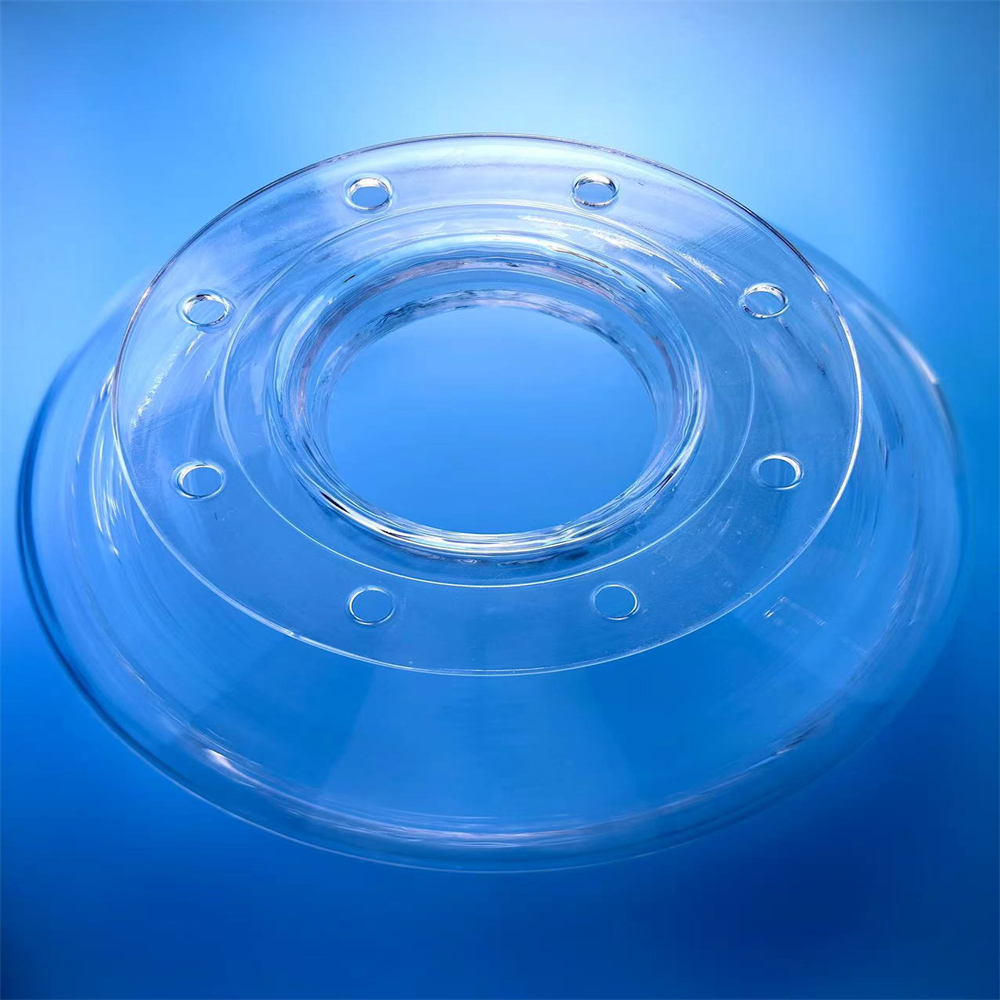
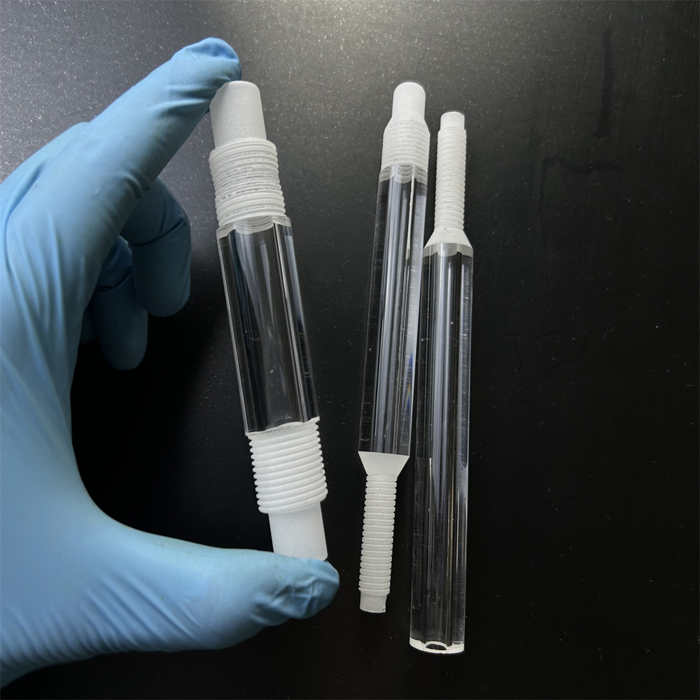
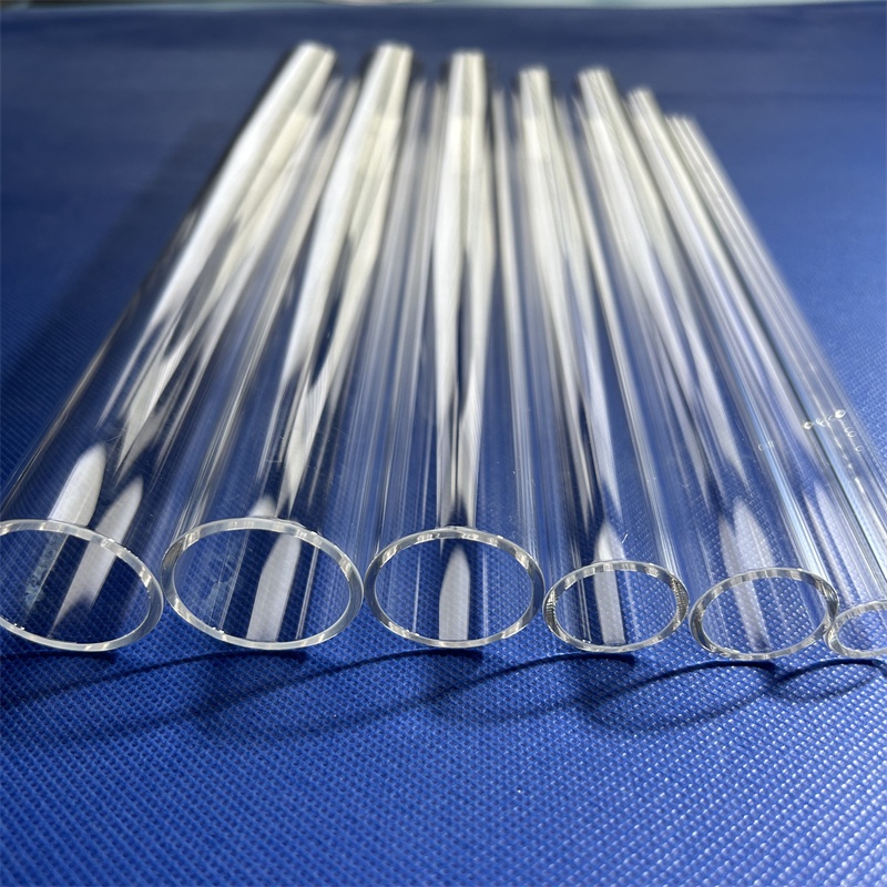
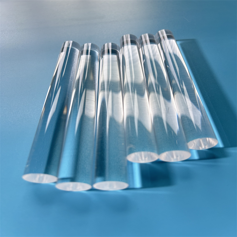
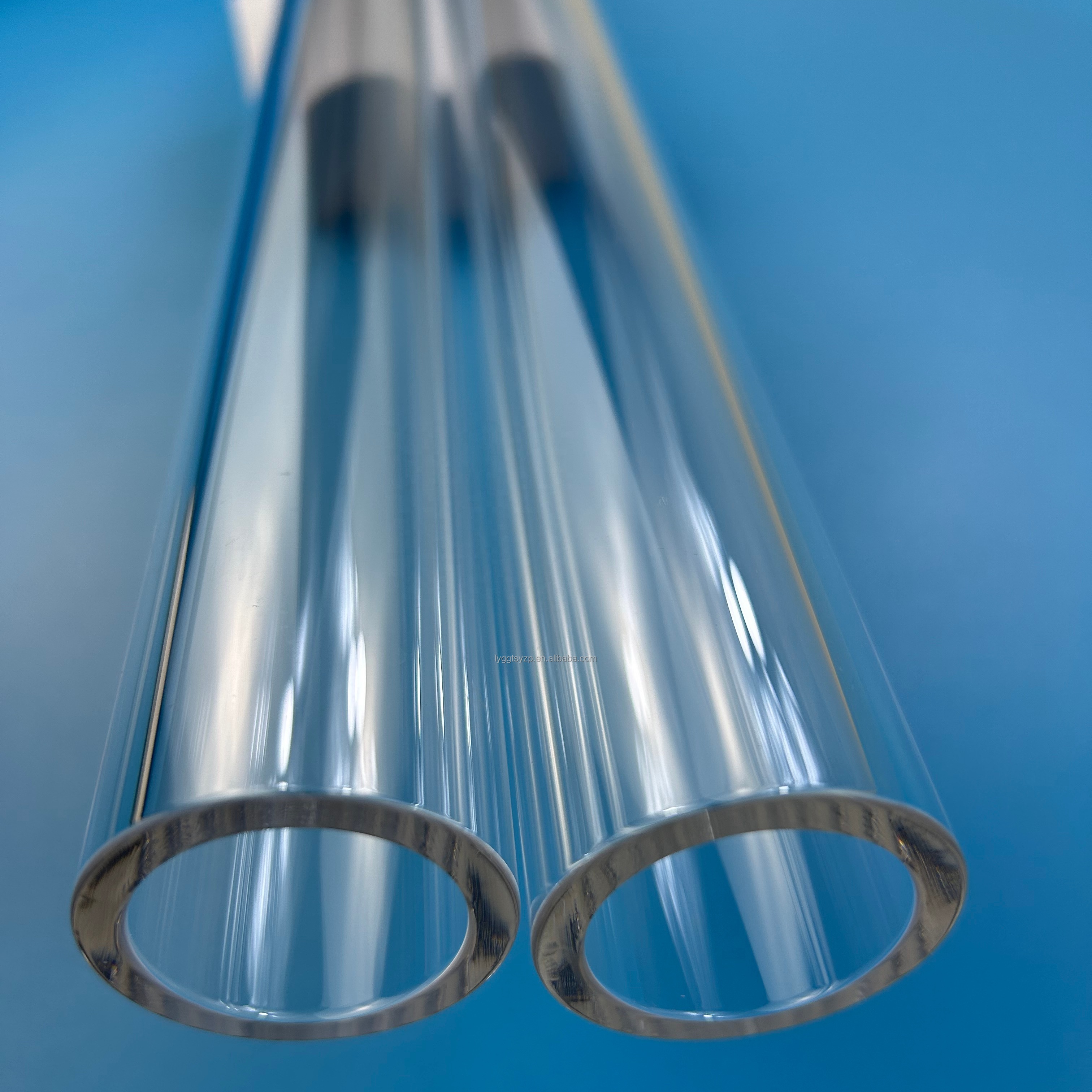
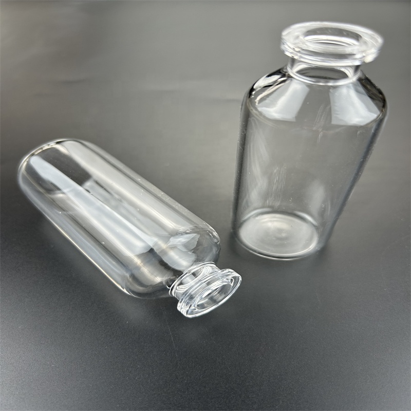
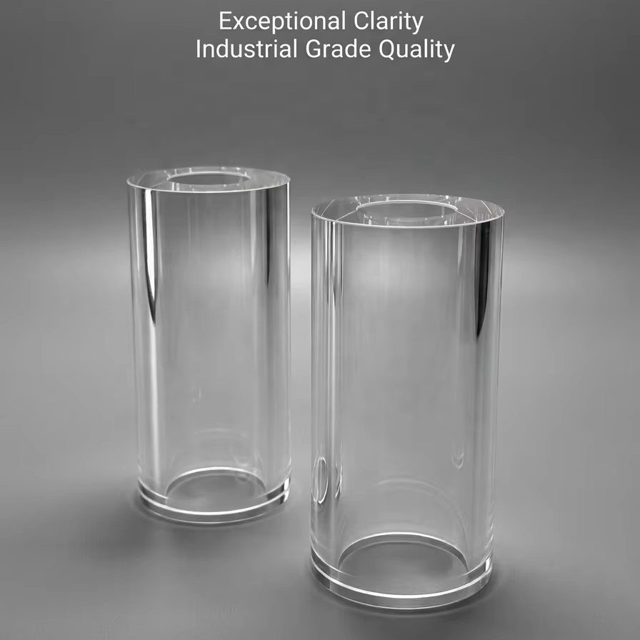
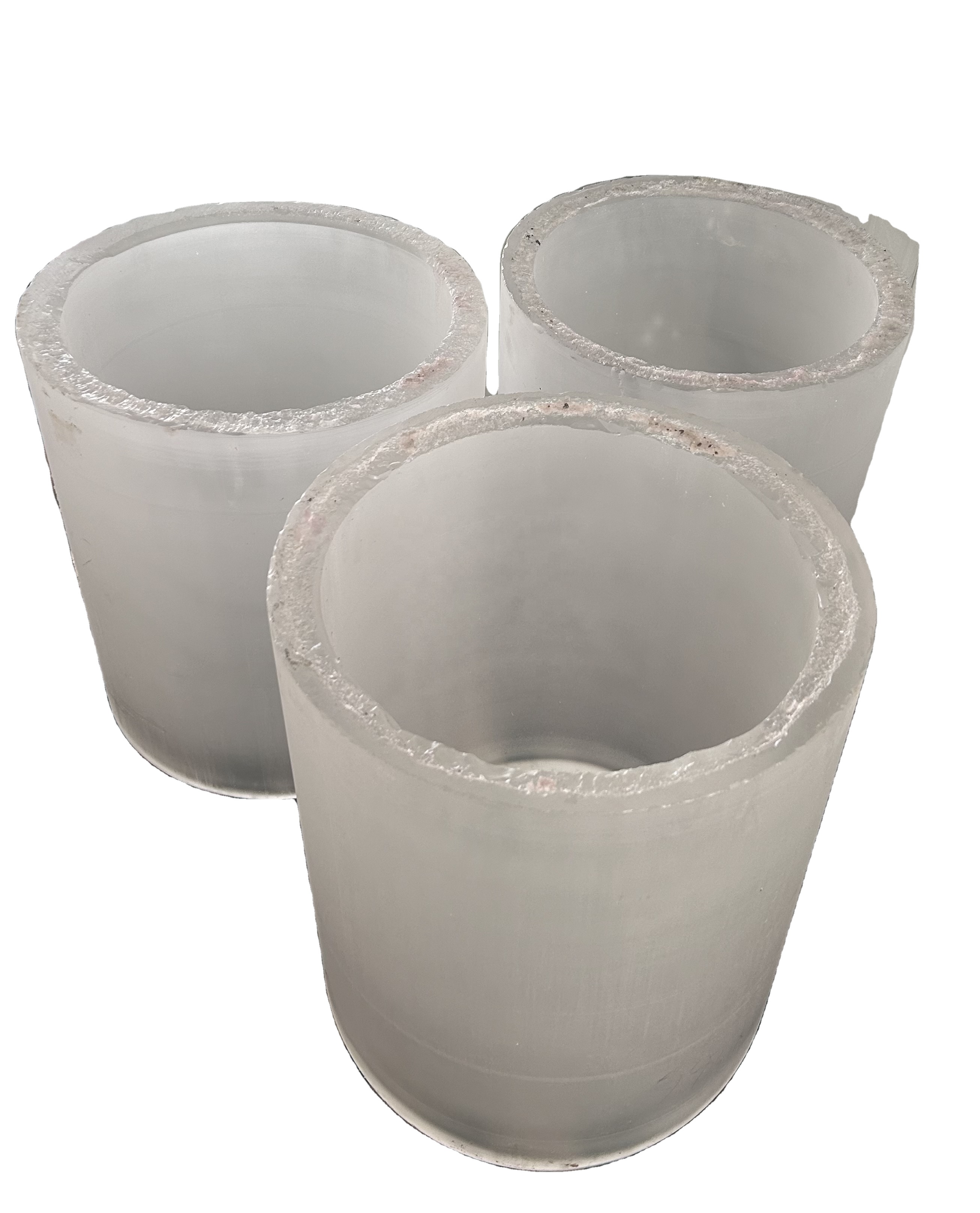
1. Technical Whitepaper: Fused Silica Substrates in Modern High-Tech Industry
In the rapidly advancing domains of semiconductor fabrication, deep-ultraviolet (DUV) optics, photovoltaic wafer processing, and microfluidics, Fused Silica Substrates represent a fundamental material class required for extreme thermal, chemical, and optical performance. Unlike standard borosilicate or soda-lime glasses, fused silica is an amorphous form of silicon dioxide (SiO₂) produced through chemical synthesis or by melting naturally occurring high-purity quartz crystal.
When procurement managers and optical engineers evaluate a China wholesale fused silica substrate supplier, understanding the microstructural, optical, and thermal variance between synthetic fused silica (JGS1), optical grade fused quartz (JGS2), and infrared grade quartz (JGS3) is critical for matching material specs to operational stress levels.
Material Classification & Optical Transmission Spectrum
The performance of a fused silica substrate is primarily governed by its trace impurity levels (measured in parts per billion or ppb) and its hydroxyl group (OH⁻) content:
| Material Grade | Raw Material Source | OH⁻ Content (PPM) | Primary Spectral Transmission Range | Typical Industrial Applications |
|---|---|---|---|---|
| JGS1 (Synthetic Fused Silica) | Silicon Halide Synthesis (SiCl₄) | 500 - 1500 PPM (High OH) | 185 nm – 2500 nm (Deep UV & Visible) | DUV Lithography, Laser Windows, Semiconductor Wafers, UV Spectroscopy |
| JGS2 (Fused Quartz) | Refined Natural Quartz Crystal | 30 - 150 PPM (Medium OH) | 220 nm – 2500 nm (UV & Near IR) | CVD Boat Covers, Furnace Sight Glasses, Industrial Substrates |
| JGS3 (Infrared Fused Silica) | Vacuum Fusion Process | < 5 PPM (Low OH) | 260 nm – 3500 nm (Infrared & Thermal) | IR Optical Sensors, High-Temperature Inspection Windows, CO₂ Lasers |
Physical, Thermal & Mechanical Properties Matrix
| Physical Parameter | Measured Value | Engineering Significance |
|---|---|---|
| Density | 2.20 g/cm³ | Lightweight structural optical support |
| Coefficient of Thermal Expansion (CTE) | 5.5 × 10⁻⁷ / K (20°C to 320°C) | Near-zero thermal deformation under extreme thermal shock |
| Continuous Operating Temperature | 1100 °C | Stable operation in high-temp diffusion furnaces |
| Peak Short-Term Temperature | 1300 °C | Resists thermal spikes without structural failure |
| Dielectric Strength | 10 kV/mm (at 20°C) | Exceptional electrical insulation for semiconductor plasma chambers |
| Mohs Hardness | 5.5 – 6.5 | High scratch resistance; requires diamond grinding & CMP polishing |
| Surface Roughness (Polished) | Ra < 0.5 nm (Sub-nanometer) | Minimizes laser light scattering in optical applications |
Why Engineering Teams Partner with Zelvo Quartz
Located in Donghai County, Jiangsu—China's world-renowned quartz hub—Lianyungang Zelvo Quartz Products Co., Ltd. integrates direct raw material access with high-precision CNC machining.
Drawing-Based Custom Fabrication
Complete machining capabilities including laser drilling, micro-grooving, wafer slotting, edge chamfering, flame polishing, and precision CNC milling based on 2D STEP/CAD files.
Rigorous E-E-A-T Quality Control
100% optical transmission testing, strain viewer birefringence inspection, and dimensional verification before dispatch. Full material traceability certificates provided upon request.
Rapid Turnaround & 1-Piece MOQ
Supporting R&D laboratories and OEM manufacturers with low-volume prototyping from 1 piece to scalable wholesale batch supply with fast dispatch windows.
2. Future Procurement Trends in Fused Silica & Quartz Substrates (2025–2030)
As global high-tech industries undergo major technological shifts, B2B procurement strategies for fused silica substrates are evolving rapidly. Technical buyers and supply chain managers must stay ahead of the following market trends:
1. Sub-Nanometer Surface Roughness for Semiconductor CMP & EUV Optics
With the semiconductor industry scaling toward 2nm process nodes and below, requirement for surface flatness (Total Thickness Variation or TTV < 1μm) and surface roughness (Ra < 0.2nm) on fused silica dummy wafers and optical windows has skyrocketed. Modern suppliers must employ Chemical Mechanical Planarization (CMP) and ion beam finishing to eliminate subsurface damage (SSD).
2. Rising Demand in Microfluidic & Bio-Chip Substrates
Fused silica's high optical clarity, low background fluorescence, and resistance to harsh biological solvents make it the material of choice for next-generation DNA sequencing microchips and organ-on-a-chip devices. Micro-channel etching via femtosecond laser ablation on fused silica substrates represents one of the fastest-growing wholesale custom market segments.
3. High-Power Fiber Laser Optics & Thermal Resistance
The rapid adoption of industrial laser cutters operating at 20kW to 60kW requires fused silica substrate windows with near-zero bulk absorption (< 5 ppm/cm at 1064nm). Substrates with residual stress or inclusions suffer from thermal lensing, causing focal shift and beam degradation. Sourcing low-OH, high-homogeneity fused silica has become a top priority for laser system OEMs.
4. Resilient & Direct-from-Source Supply Chains in China
Global buyers are increasingly consolidating vendor networks by partnering directly with verified primary fabricators in China's quartz clusters like Donghai. Direct sourcing minimizes intermediary markups, guarantees direct engineering feedback, and reduces production lead times for custom dimensions.
3. Manufacturing Technology Trends: Advances in Quartz Fabrication
Producing ultra-high purity quartz and fused silica substrates requires an interplay of thermal processing, chemical synthesis, and precision cold machining. Leading manufacturers in China are investing heavily in advanced technological pathways:
Femtosecond Laser Machining
Traditional mechanical diamond drilling introduces micro-fractures along edge profiles. Modern femtosecond laser processing allows cold machining of complex micro-hole arrays, slotting, and step-cuts on ultra-thin fused silica wafers without thermal strain or edge chipping.
Automated Flame Welding & Polishing
Combining robotic multi-axis hydrogen-oxygen burners with optical sensors enables flawless flame-polishing of quartz tube ends, flanges, and substrate edges. This process seals micro-cracks, vastly increasing mechanical strength and thermal fatigue resistance up to 1200°C.
Cleanroom Packaging & Surface Cleaning Protocols
Precision fused silica substrates destined for vacuum coating or semiconductor line integration undergo automated ultrasonic multi-stage detergent washing, deionized water rinsing (>18 MΩ·cm purity), and warm HEPA air drying inside Class 1000 cleanroom environments. Substrates are vacuum sealed in lint-free bags to prevent airborne particulate contamination during international transit.
Need Custom Fused Silica Substrates According to Your Drawings?
Upload your technical specifications, CAD drawings, or dimensional requirements. Our engineering team reviews feasibility and provides a factory-direct wholesale quote within 2 hours.
Get Catalog4. Frequently Asked Questions (FAQ) – Sourcing & Technical Guidance
Based on technical queries raised by global procurement officers, optical researchers, and manufacturing engineers, we have compiled detailed solutions to common fused silica sourcing challenges:
5. Enterprise Profile & Manufacturing Superiority: Zelvo Quartz
Lianyungang Zelvo Quartz Products Co., Ltd. is a specialized manufacturer and exporter of technical quartz glass and high-purity fused silica components located in Donghai County, Jiangsu Province—the primary quartz refining hub of China. Our factory spans modern thermal glass-blowing bays, automated CNC diamond machining suites, laser cutting rooms, and optical polishing workshops.
Key Operational Advantages:
- Direct Raw Material Advantage: Situated directly within the Donghai crystal region, securing ultra-pure raw quartz sand (> 99.99% SiO₂) at optimized supply cost.
- Full Spectrum Fabrication: In-house capabilities include precision cutting, grinding, laser drilling, slotting, bending, flame welding, optical polishing, and sandblasting/frosting.
- Rapid Technical Communication: Direct access to experienced glassblowing technicians and optical engineers who review STEP/CAD files and respond within 2 hours.
- Global Logistics & Compliance: Experienced export management covering FOB, CFR, CIF, EXW, DDP, and DDU shipment terms to North America, Europe, Southeast Asia, and the Middle East.