Featured Quartz Glass Substrates & Precision Components
Direct-factory high-purity quartz substrates, rods, plates, and custom fabricated equipment exported worldwide.
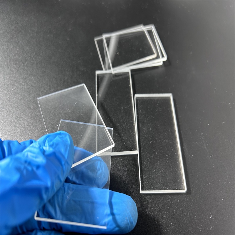
Customized High Temperature Transparent Fused Quartz Glass Sheet Welding Cutting Services Clear Plate Custom Sizes Optics Grade
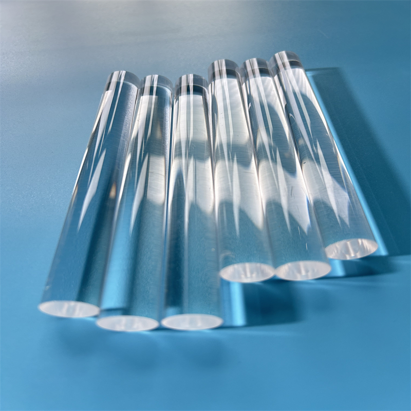
Custom Guitu Quartz GT Model High Purity Optical Quartz Light Guide Cylinder Rod 99.99% SiO2 for Optical/Semiconductor
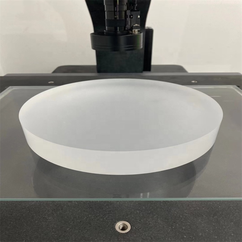
Custom Size Clear Fused Quartz Plate Premium Quality High Temperature Resistance (1100C) Glass Sheet for Optics Welding
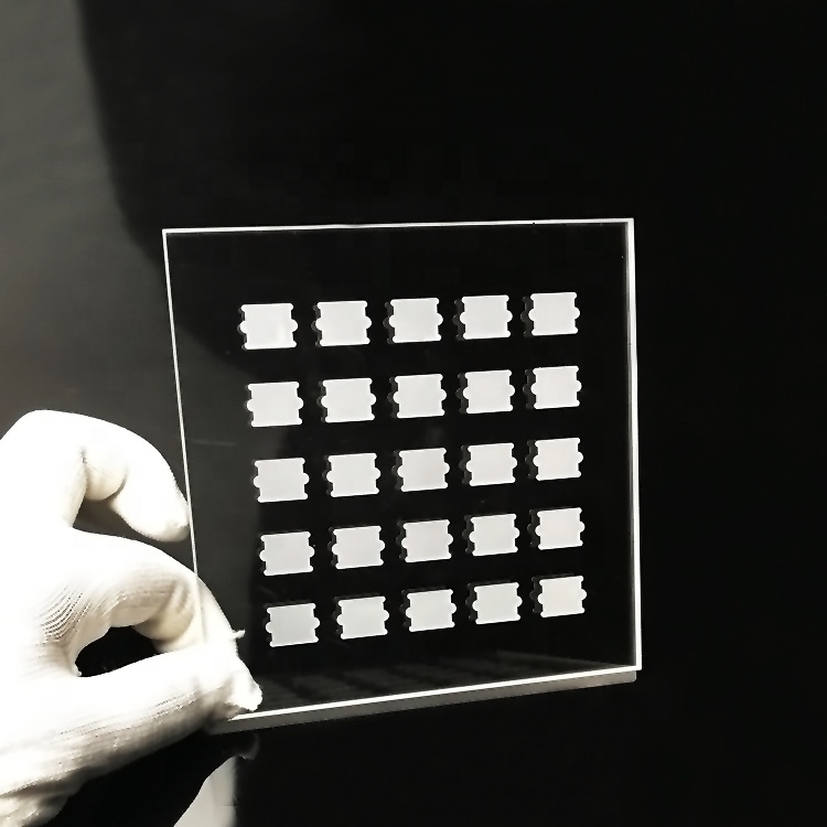
Factory Custom Fused Quartz Glass Circular High Quality High Temperature Welding Cutting XRD Sample Holder Optics Clear
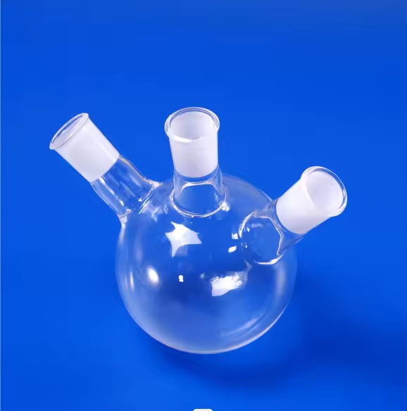
High Temperature Resistance Transparent Quartz Glass Twin Tube Bottom Flask Bending/Welding/Cutting/Moulding Services Lab Use
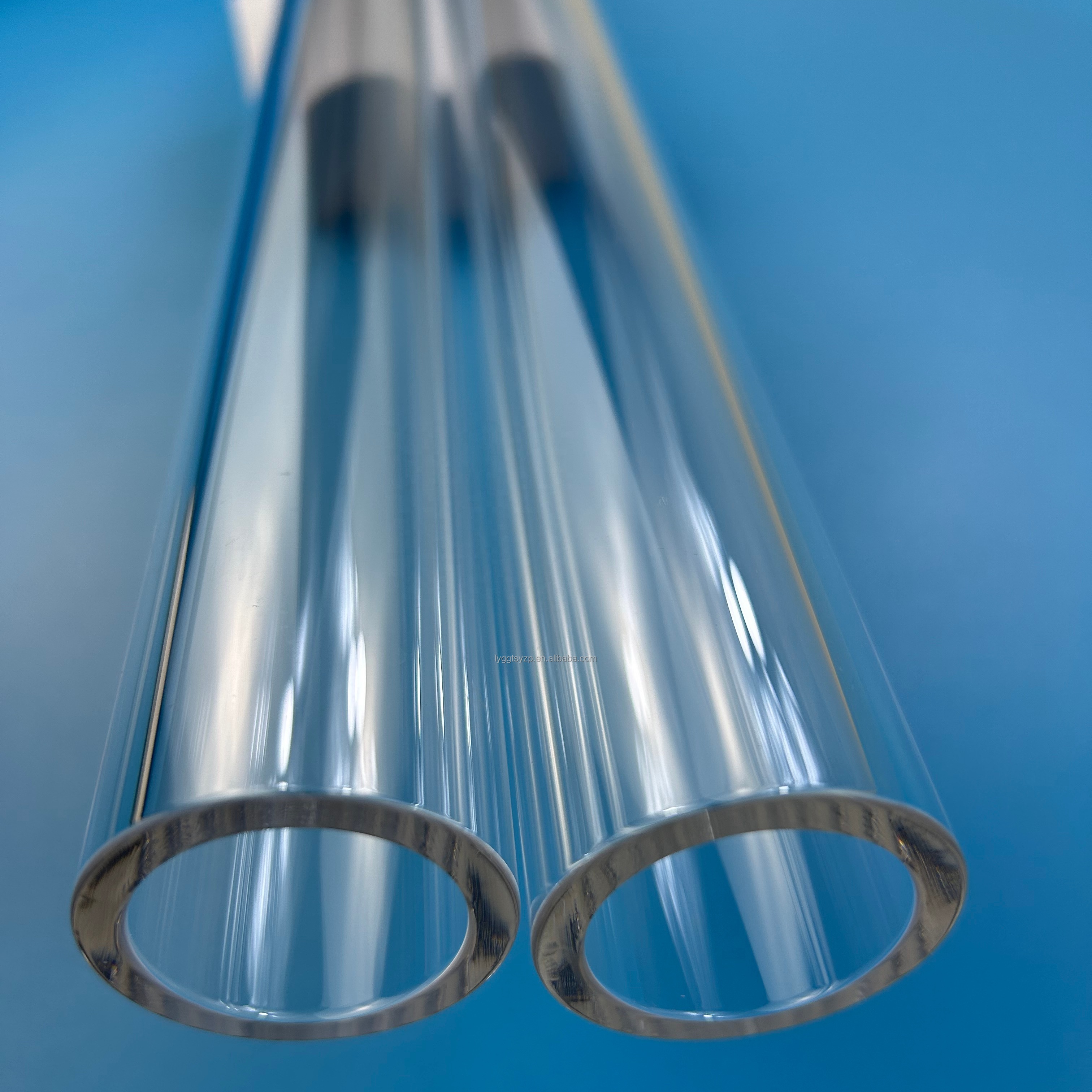
Polished Clear Quartz Twin Tube Ozone Free Heater Chemical Lab Equipment Semiconductor Furnace Tubes Welding Moulding Bending
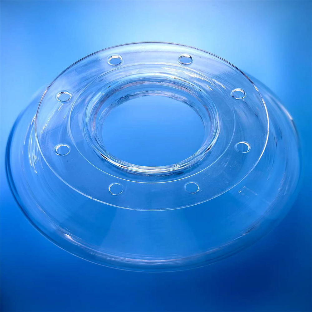
Customize Size Thickness Twin Tube Clear High Purity Flange Quartz Tube Fused Silica Polished Flange Ring Bending Welding
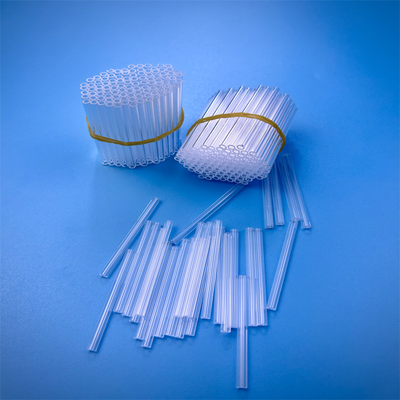
High Quality Transparent U-Bent Quartz Glass Tube Bending/Cutting/Welding Services 99.99% Pure Quartz Ozone Free Polished
Comprehensive Technical Whitepaper: High-Purity Fused Quartz Substrates in Modern Industry
As semiconductor node scaling advances beyond 3nm and optical power densities reach petawatt thresholds, the technical requirements for foundational substrate materials have escalated exponentially. Fused quartz substrates—manufactured through the high-temperature melting of natural silica crystals or chemical synthesis—serve as critical enablements across wafer manufacturing, photolithography mask blanks, deep ultraviolet (DUV) optics, and chemical vapor deposition (CVD) high-temperature processing.
Information Gain Insight: While standard optical glass (such as N-BK7 or Borosilicate) degrades under high thermal flux or ultraviolet exposure, fused quartz demonstrates near-zero thermal expansion coefficient ($5.5 \times 10^{-7} / ^\circ\text{C}$), extreme chemical inertness to acids, and exceptional broadband spectral transmission from 190 nm (DUV) to 3500 nm (Near-IR).
Material Classification & Optical Grade Matrix
Understanding the exact chemical and structural characteristics of quartz glass is vital for B2B engineering procurement teams. Material selection determines substrate longevity, optical wave-front distortion, and laser damage threshold (LDT):
| Quartz Grade Code | Material Origin | SiO₂ Purity | OH⁻ Content | Primary Industrial Applications |
|---|---|---|---|---|
| JGS1 (UV Fused Silica) | Synthetic Silicon Tetrachloride ($SiCl_4$) | ≥ 99.9999% | 50 - 2000 ppm | DUV Optics, Excimer Laser Windows, Photolithography Mask Substrates |
| JGS2 (Optical Quartz) | Refined Natural Quartz Crystal | ≥ 99.99% | 30 - 100 ppm | Precision Mirrors, Optical Windows, Spectroscopy Substrates |
| JGS3 (Infrared Quartz) | Electrically Fused Quartz | ≥ 99.99% | < 5 ppm | Infrared Windows, High-Temperature Furnace Viewports, Thermal Shields |
Physical, Thermal & Electrical Performance Metrics
Our exported quartz substrates undergo rigorous physical validation. Below are verified engineering benchmarks for key structural applications:
- Density: $2.20 \text{ g/cm}^3$ providing high strength-to-weight ratio in aerospace optical windows.
- Mohs Hardness: 5.5 to 6.5, providing superior wear resistance during automated CMP handling.
- Softening Point: Approximately $1683^\circ\text{C}$; Annealing Point at $1215^\circ\text{C}$; Continuous working limits up to $1100^\circ\text{C}$.
- Dielectric Strength: $25-40 \text{ kV/mm}$ at room temperature, ideal for high-voltage dielectric isolation wafers.
- Thermal Shock Resistance: Capable of withstanding rapid temperature drop from $1000^\circ\text{C}$ into room-temperature water without micro-cracking.
Why Partner With Lianyungang Zelvo Quartz?
Located in Donghai, Jiangsu—China's premier quartz manufacturing capital—we combine local raw material dominance with ultra-precision CNC and laser processing capabilities.
Drawing-Based Custom Fabrication
From 2D CAD sketches to 3D STEP models, our master glassblowers and CNC technicians execute custom laser drilling, grooving, slicing, edge chamfering, and flame polishing with tight tolerances ($\pm 0.01\text{ mm}$).
Strict Trace Impurity Control
Using high-purity washing techniques and Class 10,000 cleanroom packaging, heavy metal trace elements (Al, Fe, Ca, Na, K) are maintained below strict industrial thresholds (< 20 ppm total) to eliminate semiconductor process contamination.
Rapid Prototyping & MOQ 1 PC
We eliminate high minimum order barriers for research laboratories, university incubators, and specialized B2B OEMs. Prototype custom quartz substrates or sample test plates starting from a single unit.
Worldwide Shock-Proof Delivery
Custom multi-layer foam cutouts combined with ruggedized wooden crates guarantee 100% damage-free international transit via DHL, FedEx, air freight, or ocean container under flexible DDP, CIF, FOB terms.
Global B2B Procurement Trends & Market Analysis (2025 – 2030)
The global demand for high-purity quartz glass substrates is entering a structural growth phase driven by four key industrial mega-trends:
1. Semiconductor Wafer Size Expansion & Advanced Packaging
As 300mm wafer fabrication facilities upgrade process tooling, quartz components used inside diffusion furnaces, epitaxy chambers, and etching systems must meet elevated mechanical flatness standards. Substrates utilized as carrier wafers require sub-micron surface roughness ($Ra < 0.5\text{ nm}$) and minimal Total Thickness Variation ($TTV < 2\ \mu\text{m}$) to prevent focal displacement during laser stepper processes.
2. Photovoltaic N-Type TOPCon & Heterojunction (HJT) Upgrades
Solar cell manufacturing is shifting rapidly from PERC to N-type TOPCon and HJT architectures. This transition demands quartz boats, process tubes, and rectangular quartz substrates capable of enduring higher thermal cycles and corrosive gas environments ($POCl_3$ and silane) without devitrification or structural deformation.
3. High-Power Fiber Laser Optics & Quantum Photonics
With industrial laser cutting tools exceeding 30 kW output power, traditional optical window glasses melt or warp due to thermal lensing. Synthetic fused silica substrates with ultra-low OH- content offer minimal absorption coefficients at 1064 nm, driving massive adoption in laser processing heads, optical isolators, and quantum sensor substrate bases.
4. Supply Chain Resilience & Direct China Exporter Sourcing
Procurement directors in Europe, North America, and Southeast Asia are increasingly diversifying away from regional intermediaries to partner directly with primary Chinese manufacturers in Donghai. Direct sourcing yields 30% to 50% cost efficiencies while retaining strict quality assurance certified under international ISO frameworks.
Technological Evolution: Modern Processing & Quality Engineering
Producing optical-grade quartz substrates involves sophisticated cold-machining and thermal annealing processes. Below is the technical breakdown of our manufacturing workflow:
| Processing Stage | Technique Applied | Technical Objective & Parameter |
|---|---|---|
| Raw Ingot Slicing | Diamond Wire Sawing | Controlled slicing pitch to ensure minimal sub-surface damage (SSD < 15 µm). |
| CNC Shape Machining | 5-Axis CNC & Laser Micro-drilling | Precision pocketing, edge chamfering, and micro-hole drilling ($\Phi \ge 0.2\text{ mm}$). |
| Surface Lapping & CMP | Chemical Mechanical Polishing | Achieving optical surface quality up to 10/5 Scratch/Dig and flatnesses of $\lambda/10$. |
| Thermal Stress Relief | Computer-controlled Annealing Furnace | Elimination of internal residual stress to prevent birefringence and spontaneous cracking. |
| Quality Metrology | Interferometry & Spectrophotometry | Full 200 nm–2500 nm transmission curves and laser surface defect mapping. |
Frequently Asked Questions (FAQ) - Quartz Substrates Procurement
Expert answers to technical and commercial questions most frequently raised by international engineering and buying teams.
What purity level is guaranteed for your fused quartz substrates?
What is the minimum order quantity (MOQ) for custom fabricated quartz plates?
Can you fabricate quartz glass components directly from CAD drawings?
What are the continuous operating temperature limits of fused quartz glass?
How do JGS1, JGS2, and JGS3 quartz substrate materials differ?
Which international payment methods and shipping terms do you support?
How do you prevent quartz glass products from breaking during international delivery?
What quality assurance documentation is provided with wholesale orders?
Ready to Request a Custom Technical Quote?
Submit your engineered drawings or project requirements today. Our senior technical sales team will review your specifications and issue a formal quote within 2 business hours.