Featured High-Purity Quartz & Fused Silica Products
Direct Factory Export to Nagoya, Toyota City, and the Chubu Industrial Ecosystem
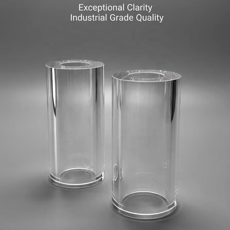
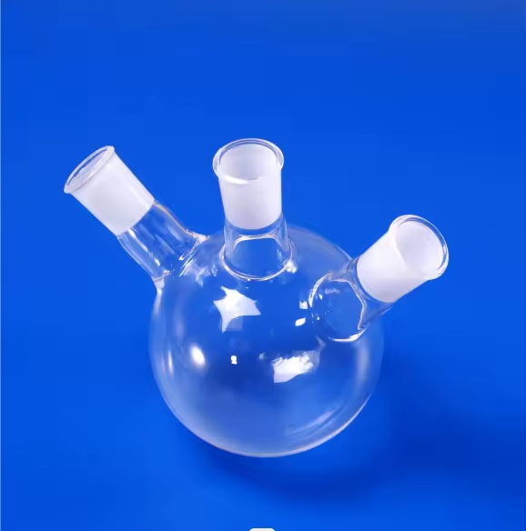
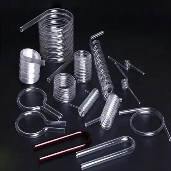
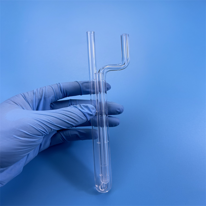
Industry Whitepaper: Fused Silica Quartz Wafer Engineering in the Nagoya & Chubu Ecosystem
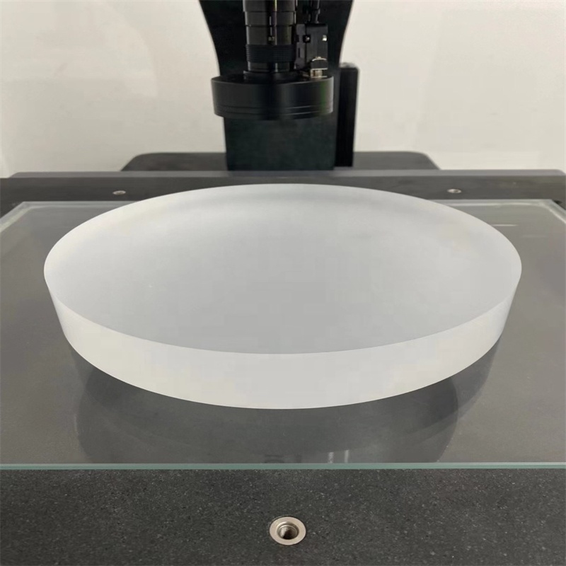
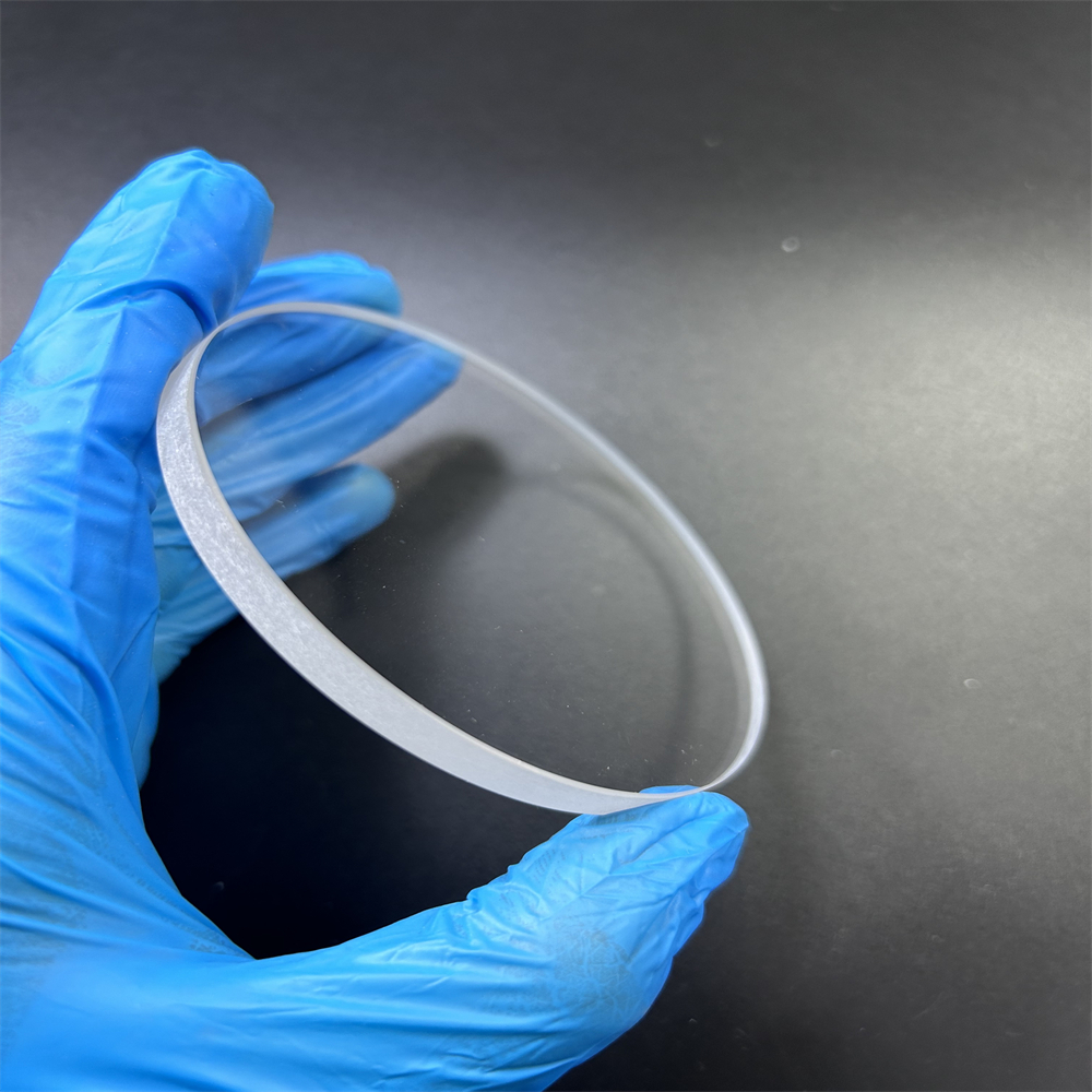
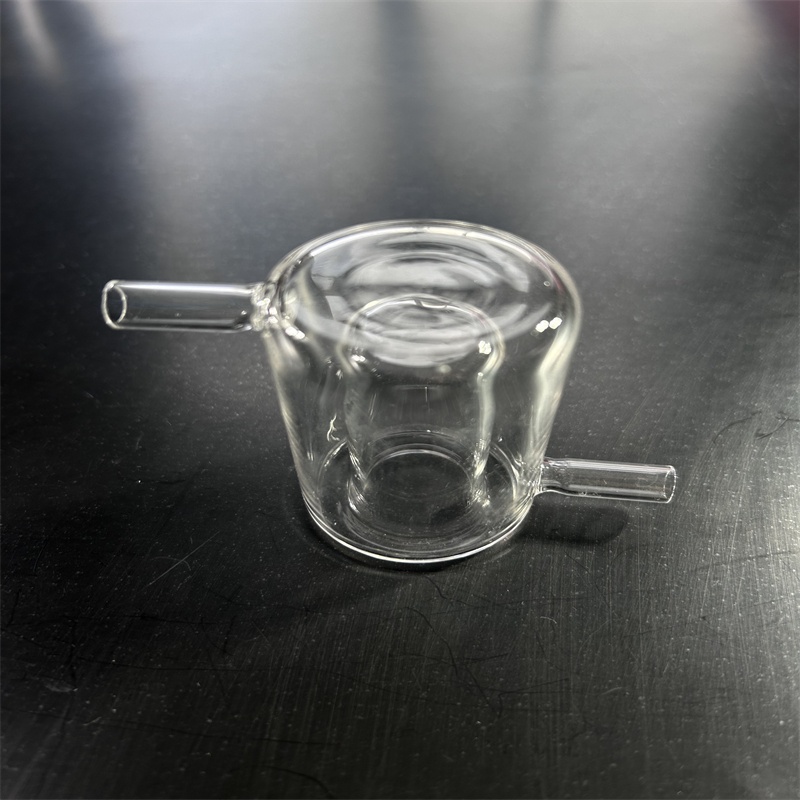
The Greater Nagoya area (Aichi, Gifu, and Mie prefectures) represents Japan’s premier manufacturing and technological powerhouse. Renowned globally for automotive excellence, precision robotics, power semiconductor fabrication, and next-generation optoelectronics, manufacturers and R&D institutions across Chubu require substrate materials capable of performing under extreme thermal, mechanical, and optical conditions. Lianyungang Zelvo Quartz Products Co., Ltd. serves as a primary China-based manufacturer and direct exporter of ultra-high purity fused silica quartz wafers, plates, and engineered quartz laboratory glassware tailored specifically for Nagoya’s high-tech industrial base.
Fused silica quartz glass is an essential material in advanced semiconductor fabrication, MEMS micro-sensor development, UV laser lithography, and high-temperature chemical vapor deposition (CVD). Engineered from high-purity silica raw materials sourced directly from Donghai, Jiangsu—China’s recognized "Crystal Capital"—Zelvo Quartz components exhibit superior optical clarity, exceptional dimensional stability, a near-zero coefficient of thermal expansion, and near-total immunity to corrosive acids.
Material Physics & Grade Classifications: Synthetic vs. Natural Fused Silica
Selecting the correct quartz substrate requires understanding the physical, optical, and chemical distinction between Natural Fused Quartz (JGS2) and Synthetic Fused Silica (JGS1). Depending on your process in semiconductor carrier manufacturing, optical windows, or analytical spectroscopy in Nagoya, material grades must be chosen according to hydroxyl (OH⁻) content, optical transmission spectrum, and trace elemental impurities.
| Physical / Mechanical Property | Standard Test Metric | Technical Value (Fused Silica Quartz) |
|---|---|---|
| SiO₂ Chemical Purity | ICP-MS Analysis | ≥ 99.99% (Optionally ≥ 99.999% for Semiconductor Grade) |
| Density | g/cm³ | 2.20 g/cm³ |
| Coefficient of Thermal Expansion (CTE) | 5.5 × 10⁻⁷ / K (20°C to 320°C) | Extremely Low Thermal Expansion (Near Zero Risk of Thermal Shock) |
| Continuous Operating Temperature | Thermal Limits | 1100 °C |
| Short-term Peak Temperature | Max Thermal Limit | 1300 °C |
| Softening Point | ASTM C338 | 1683 °C |
| Dielectric Strength | kV/mm (at 20°C) | 25 – 40 kV/mm |
| Surface Polishing Quality (Wafers) | Scratch-Dig / Flatness | 20/10 or 10/5 Scratch-Dig, Flatness < 2 μm (TTV < 2 μm) |
Localized Application Scenarios across Nagoya & Greater Aichi Industries
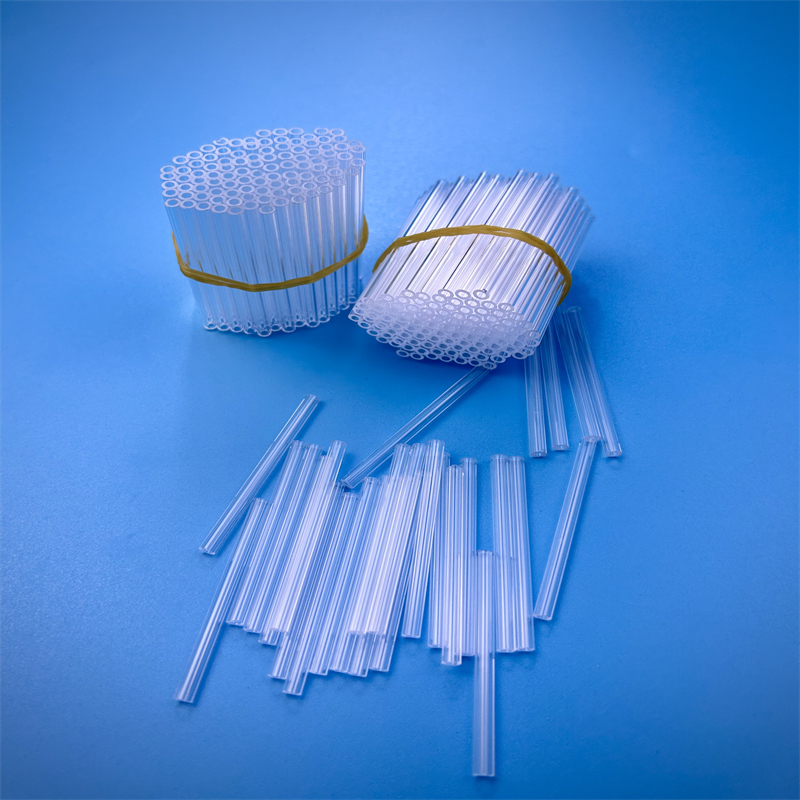
Nagoya is not merely an industrial city; it is the hub of the Chubu Economic Region, accounting for a massive share of Japan’s manufacturing output. Zelvo Quartz supplies high-precision fused silica quartz wafers, plates, and custom twin tubes specifically designed for the key industrial clusters operating in Aichi Prefecture:
Localized Market Trends Driving Quartz Wafer Demand in Chubu
Procurement requirements across the Japanese supply chain have evolved rapidly. Nagoya buyers no longer look solely for standard catalog items; they demand tightly integrated manufacturing capability, extreme traceability, and responsive customization:
- Demand for Zero-Defect Cleanroom Packaging: Japanese fab operations enforce strict micro-particle controls. Zelvo Quartz provides double-vacuum bag packaging, nitrogen flushing, and cleanroom washing (Class 100) prior to export to Nagoya.
- Miniaturization & Micro-Drilling Precision: Modern MEMS and microfluidic applications require ultra-small micro-holes, deep grooving, and stepped counterbores. Zelvo integrates automated CNC laser drilling to achieve micro-hole tolerances within ±0.01 mm.
- Rapid Prototyping Without Excessive Tooling Costs: Engineering design teams in Nagoya frequently refine prototype specs. Our 1-Piece Minimum Order Quantity (MOQ) enables cost-effective R&D trials prior to committing to mass production.
Comparative Material Matrix: Fused Silica vs. Alternative Substrates
Engineers evaluating wafer materials for optics, thermal processing, or dielectric insulation can compare fused silica quartz against common engineering glass and sapphire substrates:
| Substrate Material | Max Temp (°C) | CTE (10⁻⁶ / K) | UV Transmission | Acid Resistance | Cost Efficiency |
|---|---|---|---|---|---|
| Fused Silica Quartz (JGS1/JGS2) | 1100 °C | 0.55 | Excellent (> 90% down to 185nm) | Exceptional (Except HF) | High Value / Cost-Effective |
| Borosilicate Glass (Pyrex) | 500 °C | 3.25 | Poor (< 300nm cut-off) | Moderate | Low Cost / Lower Temp Limit |
| Single Crystal Sapphire | 1900 °C | 5.80 | Very Good | Excellent | Very High Cost / Hard to Machine |
| Soda-Lime Glass | 150 °C | 9.00 | Poor | Low | Low Cost / Basic Uses Only |
Enterprise Advantages: Why Nagoya Procurement Managers Choose Zelvo Quartz
Lianyungang Zelvo Quartz Products Co., Ltd. operates state-of-the-art quartz processing equipment in Donghai, Jiangsu. Combining deep regional raw material supply advantages with advanced fabrication tech, we bridge high-end Chinese manufacturing with demanding international quality benchmarks:
Frequently Asked Questions (FAQ) – Procurement & Logistics for Nagoya Buyers
Need Custom Fused Silica Wafers or Quartz Components in Nagoya?
Submit your CAD drawings or technical specifications today. Our senior engineering team will evaluate your project and deliver a competitive factory-direct quote within 2 hours.
Get a Quote