Precision Quartz Components & Wafer Substrates
Direct factory fabrication for UK high-technology enterprises. Every component is produced with strict dimensional tolerances, fire-polished or ground edge profiles, and ultra-low internal defect metrics.
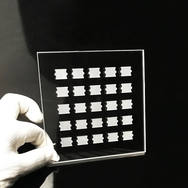
Circular Fused Quartz XRD Sample Holder Optical Clear
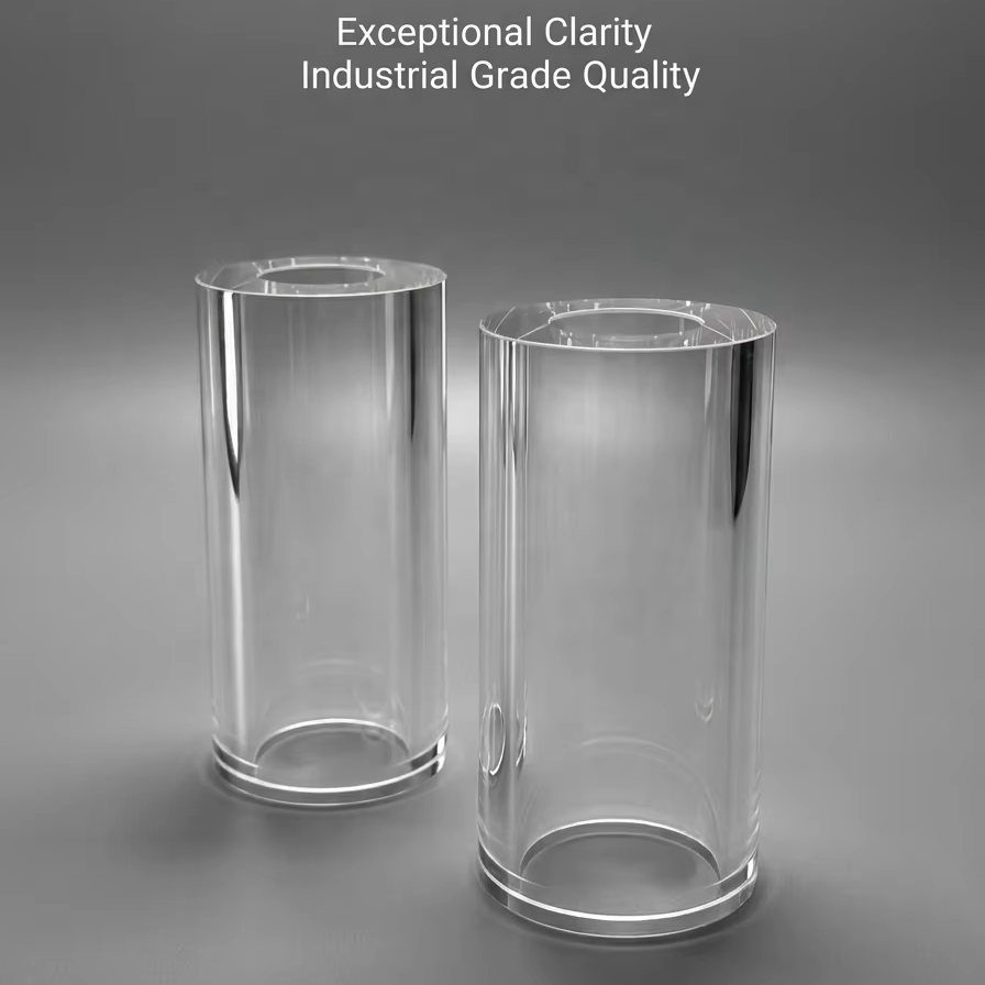
Both-Ends Polished High-Purity Quartz Twin Tube
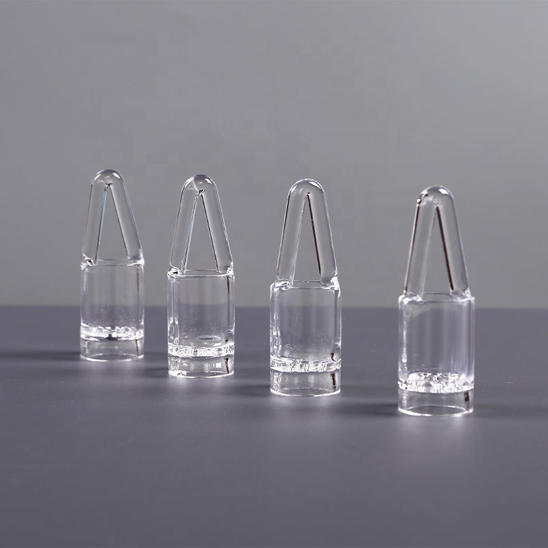
High Pressure Ozone-Free Pure Quartz Process Tube
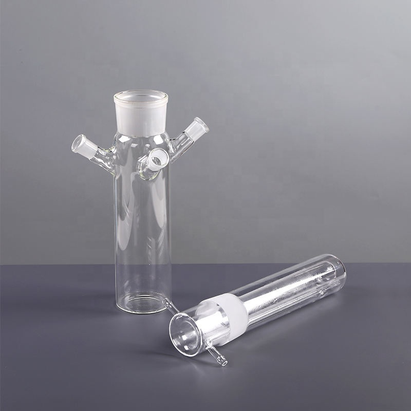
Photocatalytic Degradation Quartz Glass Reactor Container
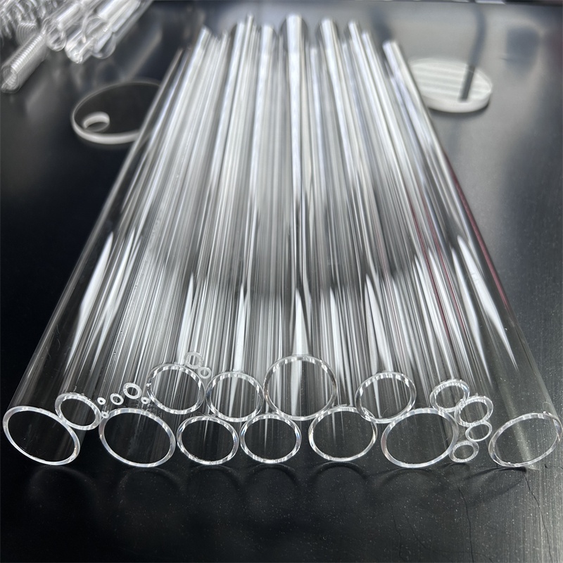
Clear Heat-Resistant 99.99% Fused Quartz Twin Tube
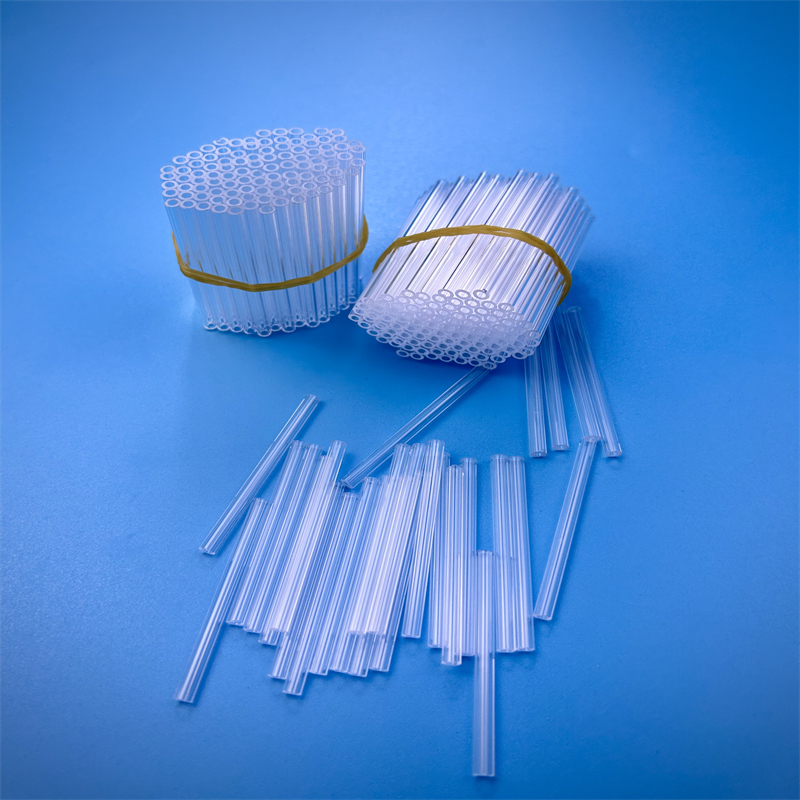
Transparent U-Bent Quartz Glass Tube Fabrications
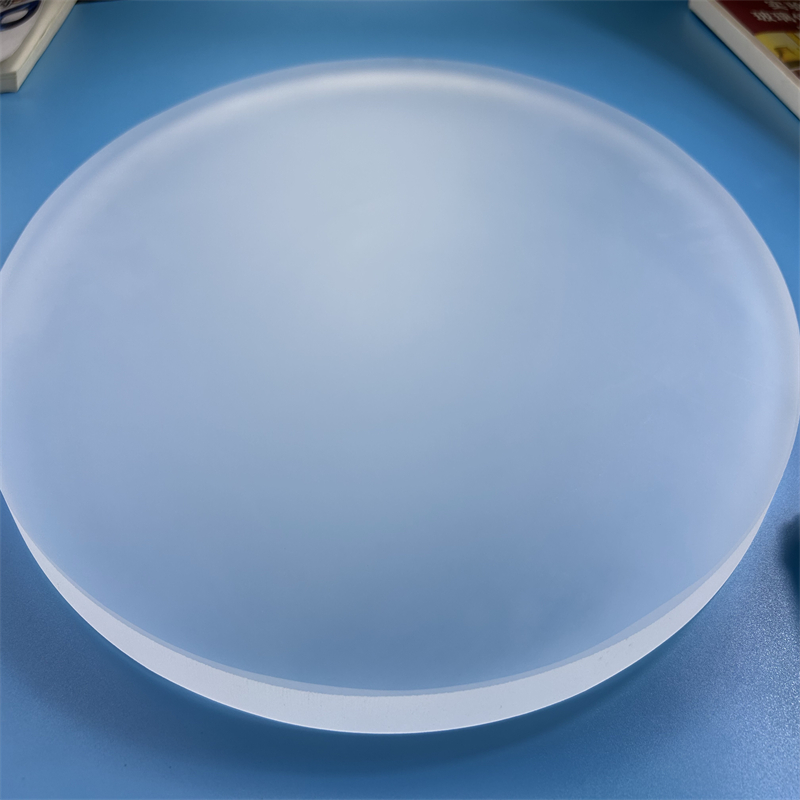
Frosted Fused Quartz Disc & Plate for Semiconductor
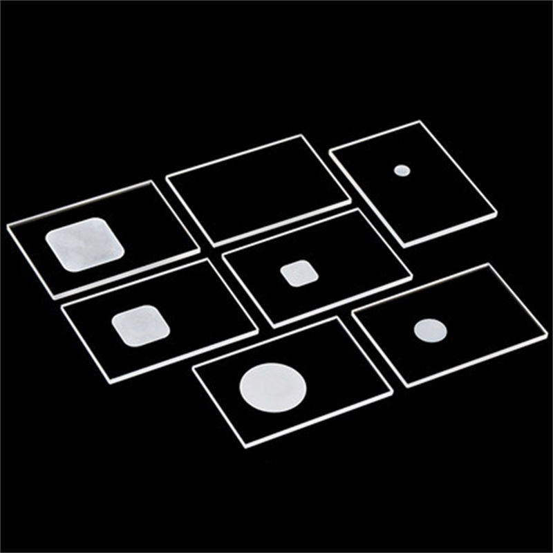
Fused Quartz Sheet Slotted Carrier for XRD Tank Testing
High-Purity Fused Silica & Quartz Wafers: Material Synthesis & Sub-Nanometer Finishing
In high-frequency electronics, integrated quantum optics, and extreme ultraviolet (EUV) lithography systems throughout the Bristol and Bath high-tech corridor, optical substrates must reconcile extreme thermal gradients with atomic-scale structural homogeneity. Standard borosilicate and soda-lime substrates fail under thermal cycling above 450°C and introduce unacceptable RF dissipation. Our OEM factory produces custom fused silica quartz wafers utilizing vapor-phase axial oxidation of high-purity silicon tetrachloride (SiCl₄), alongside electric vacuum-arc fused natural crystalline quartz from the world's most concentrated silicon deposits in Donghai, Jiangsu.
The distinction between Synthetic Fused Silica (Type III / JGS1) and Fused Natural Quartz (Type II / JGS2) governs performance metrics in critical applications. Synthetic fused silica features virtually zero metallic trace impurities (total metal content < 0.5 ppm), completely eliminating absorption bands in the Deep Ultraviolet (DUV 193 nm to 260 nm) spectrum. It exhibits an isotropic refractive index variation (Δn) as tight as 1 × 10⁻⁶, zero bubble-inclusion classification according to DIN 3140 / ISO 10110 standards, and internal stress birefringence below 2 nm/cm. For high-temperature diffusion furnaces and CVD reactor components operating up to 1150°C, electric-fused quartz delivers elevated hydroxyl (OH) resistance and superior mechanical strength against devitrification.
| Physical & Dielectric Property | Synthetic Fused Silica (JGS1 / Corning 7980 Eq.) | Optical Grade Fused Quartz (JGS2) | IR Synthetic Quartz (JGS3) |
|---|---|---|---|
| Chemical Purity (SiO₂ Weight %) | ≥ 99.9999% (< 0.1 ppm Fe, Al, Ti, Na) | ≥ 99.99% (< 15 ppm Al, < 2 ppm Fe) | ≥ 99.999% (Hydroxyl OH ≤ 5 ppm) |
| Useful Spectral Transmission Band | 185 nm – 2,500 nm (DUV / Visible) | 220 nm – 2,600 nm (UV / Visible) | 260 nm – 3,600 nm (NIR / Infrared) |
| Coefficient of Thermal Expansion (CTE, 20-300°C) | 0.52 × 10⁻⁶ / K | 0.54 × 10⁻⁶ / K | 0.55 × 10⁻⁶ / K |
| Continuous / Short-Peak Operating Temp | 1050°C / 1250°C | 1100°C / 1300°C | 1100°C / 1350°C |
| Dielectric Constant (ε) @ 10 GHz | 3.80 ± 0.05 | 3.78 ± 0.05 | 3.81 ± 0.05 |
| Dielectric Loss Tangent (tan δ) @ 10 GHz | ≤ 0.0001 | ≤ 0.0003 | ≤ 0.0002 |
| Surface Roughness (CMP Double-Side Polish) | Ra < 0.2 nm – 0.5 nm (AFM Verified) | Ra < 0.5 nm – 0.8 nm | Ra < 0.5 nm |
| Total Thickness Variation (TTV) / Bow / Warp | < 1.0 μm / < 10 μm (Ø 100mm) | < 2.0 μm / < 15 μm | < 1.5 μm / < 12 μm |
Our wafer surface finishing leverages multi-stage planetary chemical-mechanical planarization (CMP) using ultra-fine ceria and colloidal silica slurries. Cleanroom wafer dicing utilizes Nd:YVO4 diode-pumped UV laser trepanning or high-precision resin-bonded diamond blades to achieve defect-free edge chamfers (≥ 45° safety bevels according to SEMI standards M1-0307). Laser scribing and SEMI standard orientation flats or notches (100, 111, or arbitrary angles) are executed to ± 0.05 mm accuracy. Each batch destined for cleanrooms in Bristol undergoes ultrasonic multi-bath mega-sonic deionized (DI) water washing (18.2 MΩ·cm resistivity) and is vacuum-sealed in nitrogen-purged polycarbonate wafer cassettes.
Localized Application Scenarios Across Bristol & the South West
Direct OEM support for academic spinouts, cleanroom nanofabrication centers, and advanced manufacturing giants throughout the Bristol ‘Silicon Gorge’ ecosystem.
Quantum Photonics & Qubit R&D
Supporting quantum startups located around Bristol's Engine Shed and university research hubs. Our synthetic fused silica wafers serve as low-fluorescence, birefringence-free optical benches for silicon photonics, waveguide writing, and integrated single-photon detectors.
Compound Semiconductor & RF
Integrating into the South West and South Wales compound semiconductor cluster. Substrates provide near-zero RF attenuation (< 0.0001 loss tangent @ 10 GHz), essential for GaN, GaAs, and InP epitaxial growth carriers and millimeter-wave sensor packaging.
Filton Aerospace Avionics & Defense
Serving tier-1 aerospace defense primes around Filton and Severnside. Custom-annealed quartz windows, pressure vessels, and optical plates withstand 1100°C shock profiles and severe vibrational fatigue in turbine monitoring and radar radome instrumentation.
Bio-Sensors & Microfluidics
Supplying biotech incubators near Bristol Cathedral Quarter and Southmead Health research parks. Chemically inert fused silica microfluidic chips, XRD slotted carriers, and laser-drilled capillaries facilitate high-throughput genomic and cellular sequencing.
Market Trends Accelerating Quartz Adoption in Bristol
Strategic industrial shifts shaping procurement specifications across the West of England Combined Authority.
Shift to Ultra-Thin (≤ 100 μm) Wafers
Advanced microelectronics manufacturers in Bristol are adopting 3D wafer-level packaging and Through-Silicon/Quartz Vias (TQV). Demand is surging for ultra-thin 2-inch to 8-inch fused silica wafers with total thickness variation (TTV) under 1 μm to mitigate thermal mismatch in heterogeneous chiplet stacks.
Strict UK REACH & Cleanroom Circularity
Bristol companies prioritize sustainable semiconductor fabrication. Zelvo's closed-loop quartz slurry recycling, acid-free polishing chemistries, and full traceability align seamlessly with UK environmental auditing and aerospace zero-landfill mandates.
Photonic Quantum Computing Scalability
As quantum hardware progresses from laboratory demonstration to commercial rack units, optical components demand zero-defect internal purity. Synthetic JGS1 fused silica with zero bubble inclusions (Class 0 under DIN 3140) has become the gold standard across regional research labs.
Why Engineering Teams Choose Zelvo Quartz
Direct manufacturer accountability rooted in Donghai County—China's Crystal Capital—integrated with certified cleanroom fabrication and rapid global distribution.
Onsite-Verified Source
Direct factory production in Donghai, Jiangsu. Fully verified facilities eliminating middleman markups, ensuring complete material provenance from ingot to finished wafer.
≤ 2-Hour Response
Dedicated bilingual engineering project managers review 2D/3D CAD drawings (STEP, DXF, DWG) and issue thermal and tolerance feasibility analyses within 2 hours.
1-Piece Prototype MOQ
Eliminate barrier costs for university trials and pilot runs. We fabricate 1-piece custom wafer prototypes up to monthly volume runs of 50,000 units with 37% repeat client retention.
DDP Delivery to Bristol
Full logistics support including DDP, CIF, and express air freight into Bristol Airport, Heathrow, and Avonmouth port. Packaged in certified shock-absorbing cleanroom cassettes.
Frequently Asked Questions for Bristol Buyers
Clear, technically rigorous answers covering optical specs, import documentation, and factory testing protocols.
What is the fundamental difference between JGS1, JGS2, and JGS3 quartz?
Can you meet SEMI standard dimensions and custom wafer flats or notches?
What scratch-dig surface finish and flatness do you guarantee?
What are the shipping lead times and DDP terms for Bristol facilities?
How are quartz wafers protected against contamination during transit?
What quality certification and measurement data accompany orders?
Consult with Our Quartz Engineering Team Today
Have a technical drawing, specific wafer tolerance, or urgent XRD carrier requirement? Upload your design parameters or schedule an engineering consultation with our technical sales division.