Optical Grade
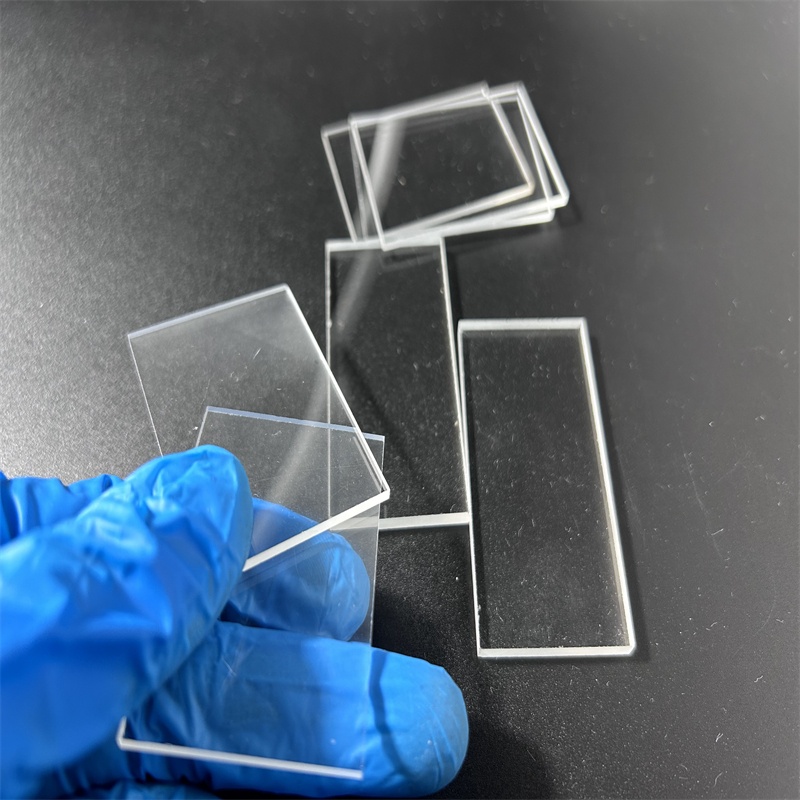
Manufactured from 99.99% to 99.999% SiO2 raw materials with superior thermal shock resistance, extreme UV-to-infrared optical transmission, and precision CNC laser profiling.
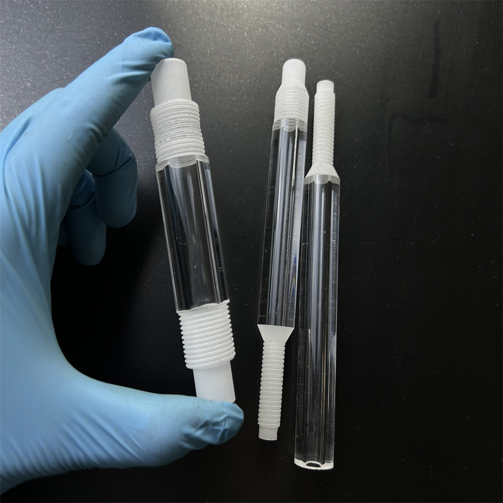
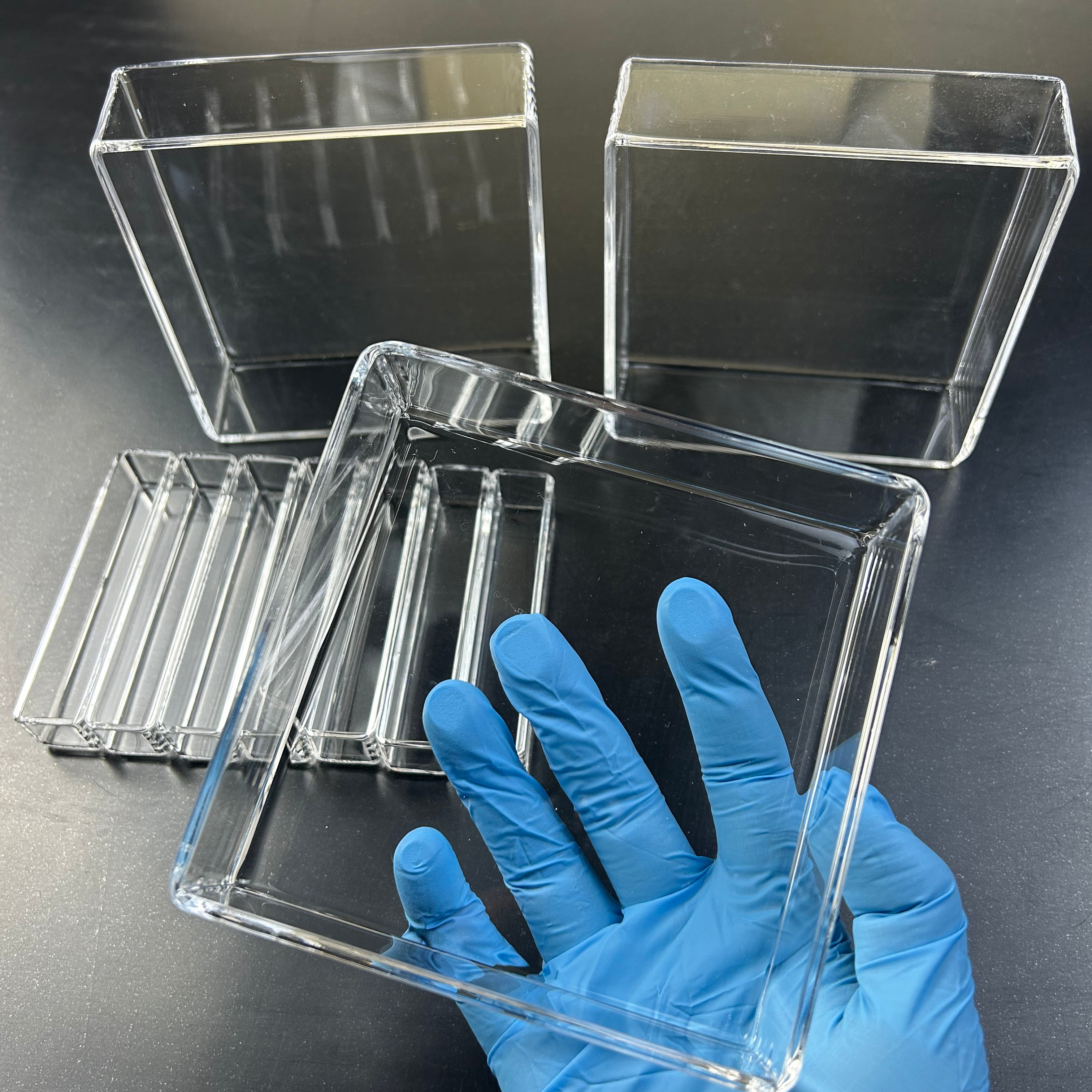
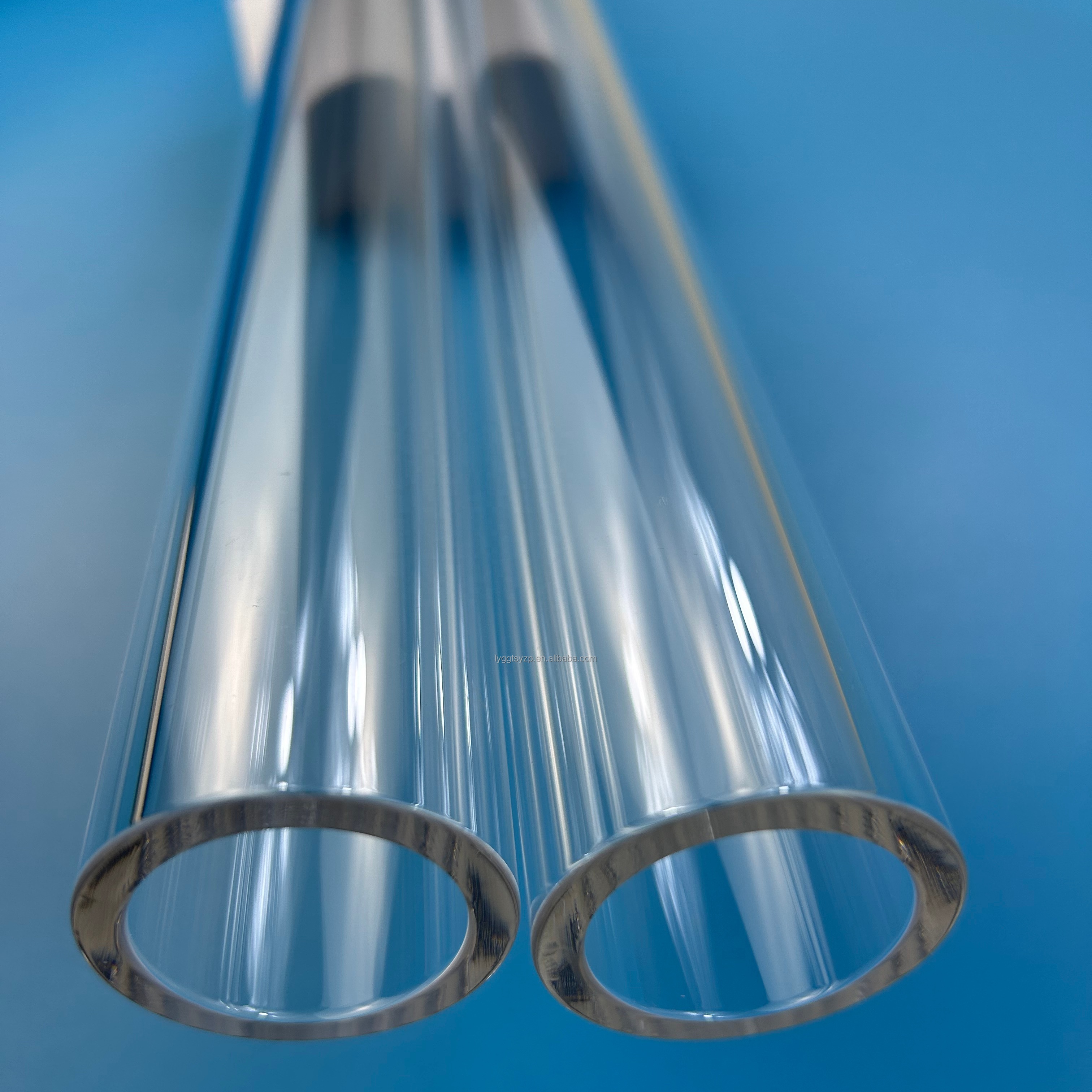
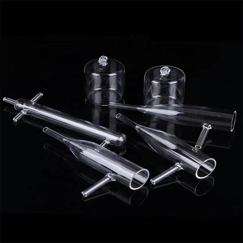
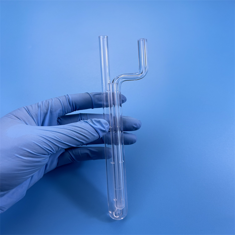
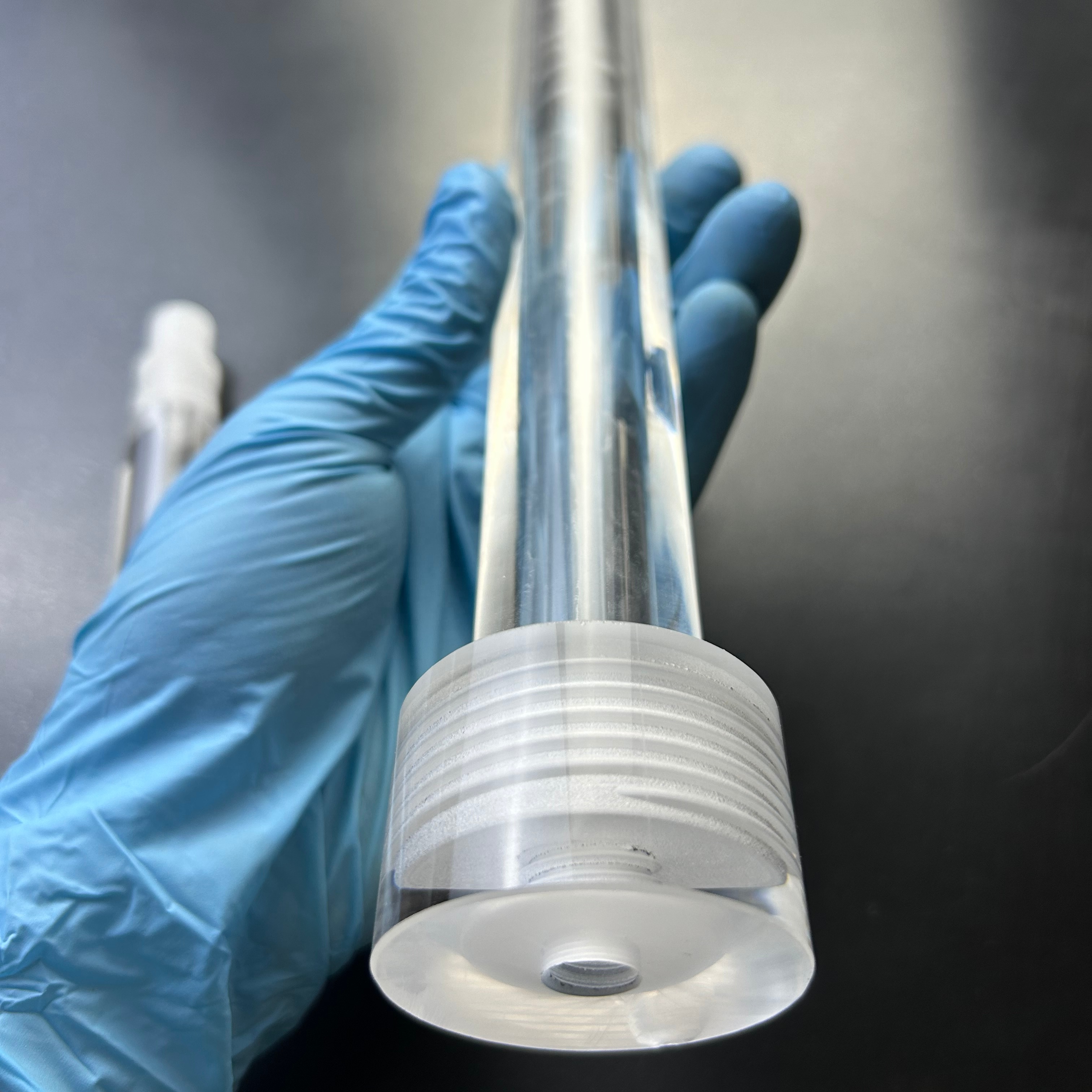
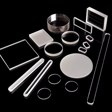
From Keihanna Science City (Kansai Science City) to the academic labs of Kyoto University and industrial clusters in Minami-ku and Fushimi-ku, our fused quartz discs address stringent mechanical, optical, and thermal boundaries.
Kyoto’s specialized semiconductor ecosystem—spearheaded by power electronics pioneers focusing on Silicon Carbide (SiC) and Gallium Nitride (GaN)—requires substrate carriers and stepper viewports with minimal thermal expansion.
Home to global precision analytical leaders such as Horiba and Shimadzu, the Kyoto area leads in molecular characterization instruments where baseline optical transmission can make or break detection thresholds.
Leading academic divisions at Kyoto University’s Katsura Campus deploy our quartz discs as thermal insulation shields and chamber viewports during chemical vapor deposition and rapid thermal processing.
Researchers within Keihanna Science City developing picosecond and femtosecond fiber lasers utilize our fused quartz optical discs as low-dispersion mirror substrates, beam splitters, and output coupler windows.
The biomedical engineering clusters at Kyoto Research Park (KRP) rely on high-purity quartz discs for fluorescence detection cells, gene sequencing microplates, and microfluidic reaction chips.
In proximity to global electronics components and ceramic capacitor powerhouses based in Kyoto and Shiga, our quartz discs serve as inert kiln furniture, wafer setter plates, and sintering separators.
An authoritative analysis of technical shifts, regulatory drivers, and domestic semiconductor manufacturing initiatives influencing material supply chains across Japan's Kansai economic sphere.
Driven by METI’s (Ministry of Economy, Trade and Industry) national semiconductor strategy, Japan’s chipmakers and Tier-1 tool fabricators are upgrading domestic wafer processing pipelines. Kyoto’s specialized niche in power modules and compound semiconductors has accelerated the migration from standard borosilicate glass to high-purity fused quartz discs capable of enduring high-density plasma deposition and atomic layer etching (ALE).
As Kyoto’s quantum computing research laboratories and extreme-UV (EUV) optical projects push sub-nanometer fabrication boundaries, the tolerance for trace metal contamination has shrunk from parts-per-million (ppm) to parts-per-billion (ppb). Procurement protocols in Kyoto now demand documented Inductively Coupled Plasma Mass Spectrometry (ICP-MS) elemental analyses for every batch of raw SiO2 fused quartz discs.
In accordance with the Kyoto Protocol’s historical legacy and the Japanese government’s 2050 Carbon Neutrality Mandate, manufacturing hubs in Kansai prioritize extended component lifecycles. Traditional furnace viewing windows degrade rapidly under aggressive thermal cycling; by selecting high-purity natural and synthetic quartz discs with near-zero devitrification rates, fabs reduce maintenance shutdowns and electrical consumption.
Engineered for precision procurement officers and optical engineers in Kyoto comparing JGS1, JGS2, and JGS3 structural and physical characteristics.
| Physical / Optical Parameter | JGS1 (Synthetic Fused Silica) | JGS2 (Optical Grade Fused Quartz) | JGS3 (Infrared Fused Silica) | Testing Protocol |
|---|---|---|---|---|
| Primary Raw Material | Synthetic SiCl4 Chemical Synthesis | Natural High-Purity Quartz Crystal | Electrically Fused Natural Quartz | Spectrochemical Assay |
| SiO2 Purity Content | ≥ 99.9999% (< 0.1 ppm impurities) | ≥ 99.995% | ≥ 99.99% | GD-MS / ICP-MS |
| Spectral Transmission Range | 185 nm – 2500 nm (Deep UV to Vis) | 220 nm – 2500 nm (UV to Near-IR) | 260 nm – 3500 nm (Extended IR) | UV-VIS-NIR Spectrophotometer |
| Hydroxyl (OH-) Content | High (800 – 1200 ppm) | Medium (100 – 200 ppm) | Low (< 5 ppm, Water-Free) | FTIR Absorption @ 2.73 µm |
| Coefficient of Thermal Expansion | 5.5 × 10⁻⁷ /°C (0 – 300°C) | 5.5 × 10⁻⁷ /°C (0 – 300°C) | 5.4 × 10⁻⁷ /°C (0 – 300°C) | Dilatometry (JIS R3102) |
| Max Continuous Temperature | 1050°C | 1100°C | 1150°C | Static Heat Test |
| Laser Damage Threshold (LIDT) | > 12 J/cm2 (1064 nm, 10 ns) | > 6 J/cm2 (1064 nm, 10 ns) | > 5 J/cm2 (1064 nm, 10 ns) | ISO 21254 Pulse Irradiation |
| Target Kyoto Application | Excimer optics, UV steppers, bio-fluorescence | Observation ports, furnace sight glasses | CO2 laser optics, IR pyrometry | System Integration |
Combining world-class raw crystal deposits from Donghai County with high-precision CNC laser trepanning, optical flat polishing, and dedicated Japanese export handling.
Equipped with ultrasonic milling, CNC 5-axis profile machining, precision laser trepanning, and diamond wire sawing. We manufacture custom circular discs, stepped flanges, bevel-edged sight glasses, and micro-holed plates holding tolerances to ±0.02 mm.
Situated in China’s Silicon and Quartz Capital (Donghai County, Jiangsu), we have unhindered access to the world’s purest natural quartz crystals. Every furnace heat is tested for trace bubble count, devitrification velocity, and residual metal elements before batch release.
We respect the iterative nature of academic research at Kyoto University and R&D prototyping across Kansai corporate laboratories. We offer zero MOQ hurdles on custom quartz discs—enabling rapid 1-piece sample verification before transitioning into batch volume runs.
Direct export protocols tailored for Japan. Multi-layered cleanroom anti-static vacuum wrapping, shock-absorbing custom foam inserts, and certified reinforced plywood crates ensure zero chipping during expedited airfreight to Kansai International Airport (KIX).
Technical clarifications addressing Japanese Industrial Standards (JIS), dimensional tolerances, surface quality, thermal hysteresis, and customs clearance procedures.
Our quartz disc fabrication adheres to the dimensional, mechanical, and optical verification procedures defined under JIS R3200 (Flat Glass Testing) and JIS R1601 (Fine Ceramics Testing). Purity certification conforms to strict SEMI and JIS standards for high-temperature semiconductor processing materials.
Depending on application requirements, we provide double-sided optical polishing delivering surface roughness Ra ≤ 0.5 nm (5 Å), with Scratch-Dig ratings of 40/20 or 20/10 (MIL-PRF-13830B). Surface transmitted wavefront flatness can be certified between λ/4 and λ/10 @ 632.8 nm using Zygo laser interferometry.
Yes. Every batch dispatched to Kyoto can include an official Certificate of Analysis (CoA) specifying ICP-MS metallic trace element measurements (Fe, Al, Ca, Mg, Ti, Cu, Na, K, Li < 20 ppm cumulative for JGS2, < 0.1 ppm for JGS1), UV-VIS-NIR spectral transmission graphs, and coordinate measuring machine (CMM) dimensional reports.
Custom prototype discs generally ship within 5 to 10 working days after 2D/3D CAD sign-off. Via express air courier (DHL, FedEx, SF Express) to Kansai International Airport (KIX), transit time to Kyoto is 2 to 4 days. We support FOB, CFR, CIF, DDP, and DAP terms, handling customs formalities with full RoHS 3 and REACH compliance declarations.
Yes. Our precision processing facility routinely fabricates stepped circular viewports, laser-trepanned counterbored holes for thermocouple feedthroughs, precision alignment notches, optical fiducial markers, and masked selective edge frosting for diffuse backlighting or seal adhesion.
We implement a strict 4-stage optical packaging standard: individual lint-free optical lens paper wrapping, secondary cleanroom anti-static PET vacuum sealing, high-density polyethylene (EPE) die-cut shock cushioning, and an exterior shock-isolated wood or heavy export carton barrier rated for drops and vibration.
Whether you require a single high-purity prototype window for a Kyoto University laboratory trial or high-volume wafer substrates for next-generation semiconductor equipment fabrication, our engineering team provides technical feasibility and quotations within 2 hours.