High-Purity Fused Silica & Quartz Solutions for Czech Engineering
From single-crystal silicon carrier wafers and UV fused silica window blanks to thermal diffusion twin tubes and XRD slotted substrates, explore our core precision quartz components manufactured in Donghai, China and exported directly to Czech enterprises.
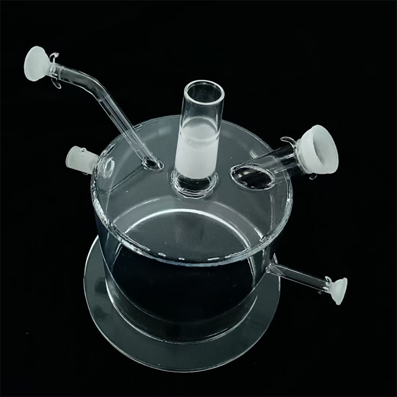
Customized High Pressure Clear Quartz Glass Tube
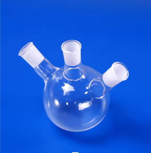
High Temperature Resistance Quartz Twin Tube Flask
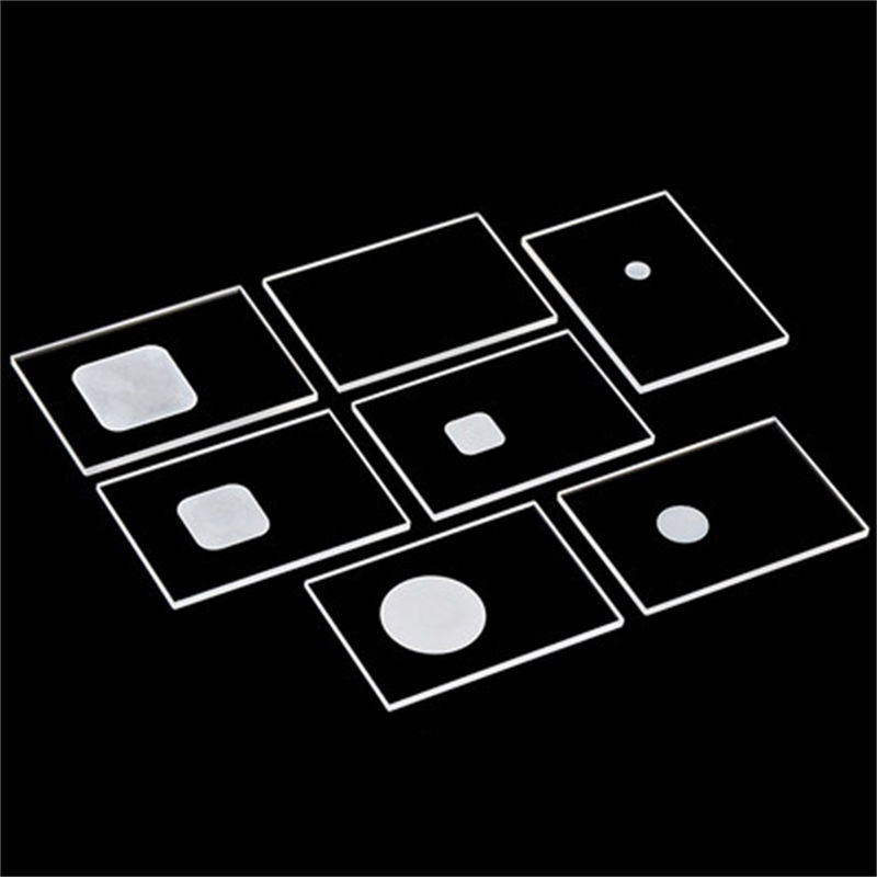
Fused Quartz Glass Sheet for XRD Sample Tank
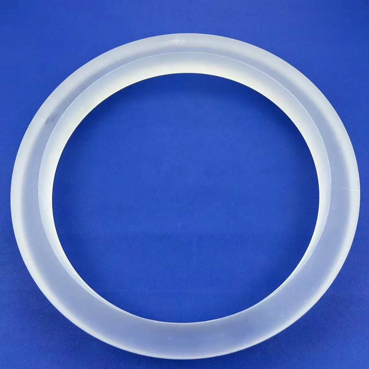
Custom Coated 99.99% Pure Quartz CVD Rings
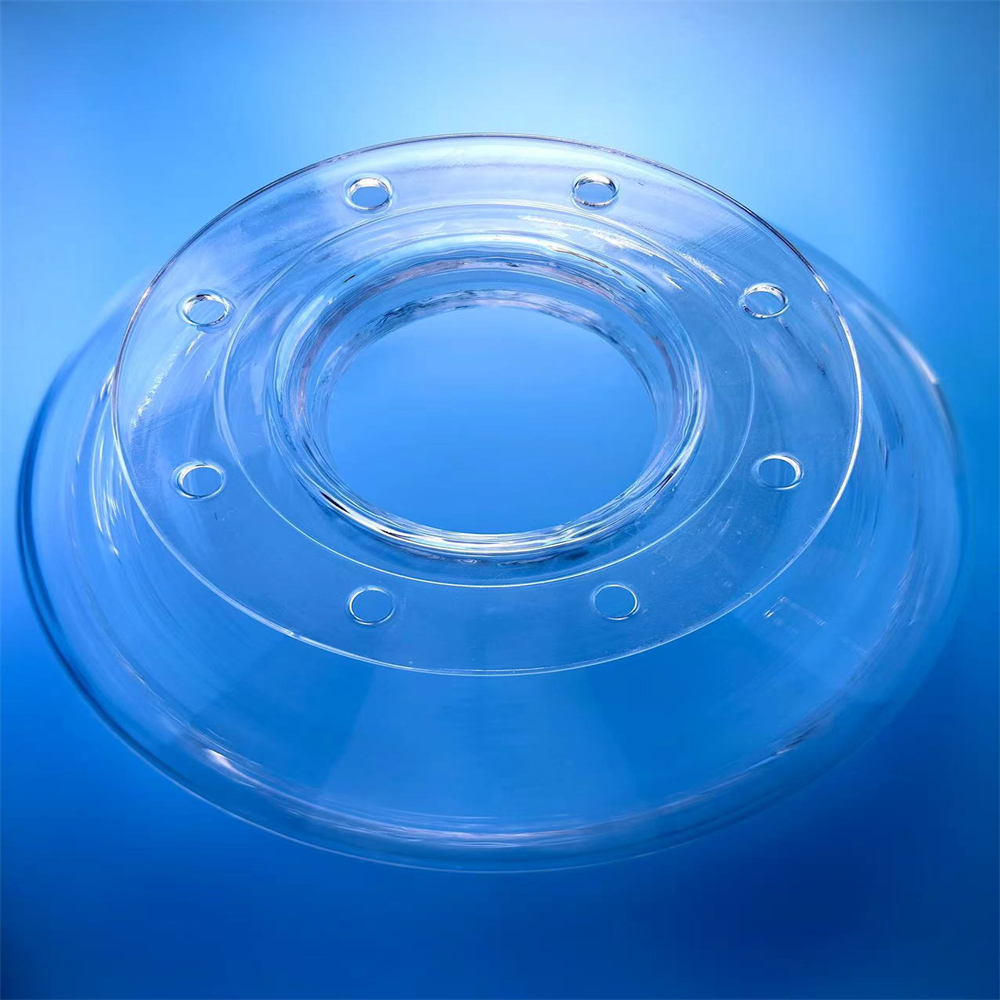
High-Purity Flanged Twin Quartz Tube
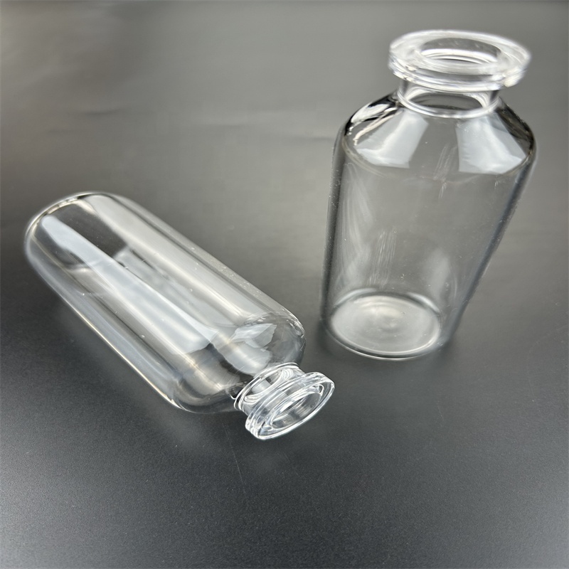
Medical-Grade Ozone-Free Quartz Ampoules
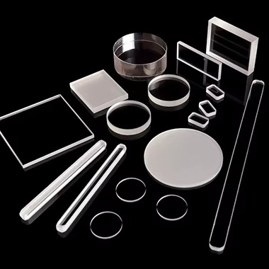
Optical Fused Silica Glass Sheet / Wafer Blank
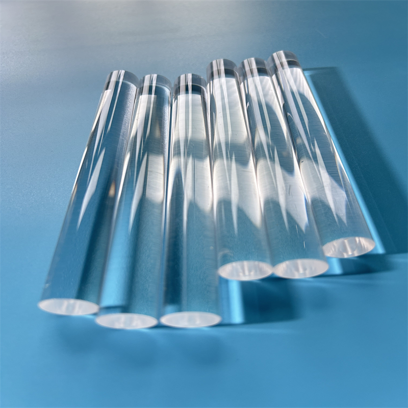
High Purity Optical Quartz Light Guide Rod
Engineering High-Purity Fused Silica Substrates for the Czech Republic’s Industrial Frontier
As the Czech Republic cements its leadership within Central and Eastern Europe's microelectronics, quantum photonics, and high-power laser physics sectors, the demand for precision fused silica quartz wafers has experienced exponential growth. Modern semiconductor fabrications in South Moravia, laser development centers in Central Bohemia, and analytical instrumentation manufacturers in Prague require substrate materials engineered to extreme physical, chemical, and optical tolerances. Zelvo Quartz, manufacturing from Donghai County—the crystal material epicenter of China—delivers an integrated OEM export channel that circumvents European third-party distributor markups while guaranteeing atomic-level substrate metrology.
Sourcing fused quartz and fused silica wafers from China to the Czech Republic requires deep technical transparency. Standard commercial quartz glass exhibits trace bubble populations and hydroxyl (OH⁻) absorption bands that compromise high-damage threshold laser optics. Zelvo Quartz eliminates these engineering risks by segregating raw boules into distinct optical tiers: JGS1 (Synthetic Fused Silica for DUV-VIS transmission down to 185 nm), JGS2 (Electric-Fused Quartz for high-temperature furnace carriers and MEMS substrates), and JGS3 (Infrared-optimized, water-free quartz transparent past 3.5 μm). By managing the entire vertical chain—from boule ingot slicing and laser trepanning to multi-stage CMP double-side polishing—we empower Czech procurement engineers to source drawing-exact substrates directly from the factory floor.
Atomic Flatness & TTV
Double-side CMP polishing achieves Total Thickness Variation (TTV) ≤ 1 μm, Bow ≤ 10 μm, and Warp ≤ 10 μm on 100 mm to 300 mm wafer diameters, accommodating strict semiconductor chucking standards.
Sub-Nanometer Roughness
Surface roughness verified via atomic force microscopy (AFM) down to Ra < 0.3 nm (3 Å), with Scratch-Dig specifications reaching MIL-PRF-13830B 10-5 for zero scattered light distortion.
Direct EU Supply Chain
Certified export packaging in Class 100 cleanroom single-wafer cassettes or multi-wafer fluoroware containers, fully integrated with DDP door-to-door delivery directly to Prague, Brno, and Ostrava.
Fused Silica vs. Natural Quartz: Substrate Selection Matrix for Engineers
Czech design engineers frequently face trade-offs between optical transmission, dielectric properties, and raw manufacturing budgets. The technical matrix below compares the structural, chemical, and dimensional characteristics of our wafer substrates against traditional borosilicate float glass.
| Property Parameter | Synthetic Fused Silica (JGS1) | Thermal Fused Quartz (JGS2) | Infrared Silica (JGS3) | Borosilicate (D263/Pyrex) |
|---|---|---|---|---|
| SiO₂ Purity Ratio | ≥ 99.999% (< 5 ppm metallic) | ≥ 99.99% (< 20 ppm metallic) | ≥ 99.995% (< 10 ppm metallic) | ~81% (multicomponent) |
| Spectral Range | 185 nm – 2,500 nm (DUV-NIR) | 220 nm – 2,500 nm (UV-NIR) | 260 nm – 3,500 nm (VIS-MIR) | 350 nm – 2,000 nm (VIS-NIR) |
| Hydroxyl (OH⁻) Content | High (~1,200 ppm) | Low (< 30 ppm) | Extremely Low (< 5 ppm) | N/A |
| Thermal Expansion (CTE) | 5.5 × 10⁻⁷ /K (0–300°C) | 5.5 × 10⁻⁷ /K (0–300°C) | 5.5 × 10⁻⁷ /K (0–300°C) | 32.5 × 10⁻⁷ /K (0–300°C) |
| Continuous Max Temp | 1,100 °C | 1,150 °C | 1,100 °C | ~500 °C |
| Dielectric Constant (1 MHz) | 3.75 | 3.78 | 3.75 | 4.6 – 6.7 |
| Dielectric Loss (tan δ) | < 1 × 10⁻⁴ | < 1 × 10⁻⁴ | < 1 × 10⁻⁴ | > 30 × 10⁻⁴ |
| Standard Wafer Diameters | 2", 3", 4", 6", 8", 12", Custom | 2", 3", 4", 6", 8", 12", Custom | 2", 3", 4", 6", Custom | Standard sizing only |
| Surface Roughness (Ra) | < 0.3 nm (CMP) | < 0.5 nm (CMP) | < 0.5 nm (CMP) | ~0.8 nm – 1.2 nm |
For high-frequency telecommunications and RF packaging projects within the Brno microelectronics zone, fused silica’s minimal dielectric loss tangent (tan δ < 0.0001) guarantees zero signal attenuation up to 40 GHz. Similarly, in high-power laser optics handled by researchers in Dolní Břežany, the virtual absence of transition metal impurities (Fe < 0.2 ppm, Ti < 1.0 ppm) ensures a Laser-Induced Damage Threshold (LIDT) exceeding 15 J/cm² at 1064 nm (10 ns pulse), safeguarding multi-million euro amplification lines from catastrophic optical failure.
Deploying Fused Silica Substrates Across the Czech High-Tech Ecosystem
The Czech Republic is not merely an assembly node; it represents one of Europe's most sophisticated epicenters for electron microscopy, optical metrology, and high-frequency power electronics. Below are the key geographic and technical hubs where Zelvo Quartz components are deployed.
Extreme Laser Physics
Substrates serve as laser debris shields, ultra-low wavefront distortion beam splitters, and vacuum window ports for the ELI Beamlines petawatt-class beamlines and HiLASE diode-pumped solid-state laser systems.
Electron Optics & MEMS
Double-side polished 4-inch and 6-inch quartz wafers are utilized for anodic bonding with silicon in MEMS pressure transducers and micro-channel diagnostic flowcells used across Brno's world-leading electron microscopy manufacturers.
Semiconductor Corridor
Supporting compound semiconductor (SiC / GaN) epitaxy, our CVD quartz rings, high-purity carrier trays, and furnace tubes provide the chemical inertness needed for chemical vapor deposition in Moravian cleanrooms.
Automotive LiDAR & Sensors
Precision-diced fused silica optical windows, diffractive optical element (DOE) blanks, and UV spectrophotometer sample cells integrated into Tier-1 automotive optical sensors and academic cleanrooms at Czech Technical University (ČVUT).
Macro Trends Driving Quartz Substrate Demand in the Czech Republic
The Czech industrial landscape is undergoing a structural transformation, catalyzed by the European Chips Act and regional specialization in quantum computing, compound semiconductor fabrication, and cleanroom automation. Several macroeconomic and technological shifts directly influence how Czech technical teams procure high-purity fused silica:
Silicon Carbide (SiC) Packaging Surge
With multi-billion-dollar expansions occurring in Rožnov pod Radhoštěm for next-generation EV power chips, the need for high-temperature carrier wafers capable of withstanding rapid thermal annealing (RTA) cycles exceeding 1,000°C without warpage has surged.
Quantum Photonics & Integrated Circuits
Czech universities and research institutes are aggressively developing photonic integrated circuits (PICs). Fused silica wafers with near-zero fluorescence and extreme broadband UV-to-NIR transmission serve as the foundational backplane for on-chip waveguiding.
Decoupling from Middleman Markup
Historically, Czech labs relied on regional optical re-sellers with 300% to 500% price markups and 12-week lead times. Direct factory procurement from verified Chinese manufacturers with standard SEMI-wafer stocks resolves budget limitations for Horizon Europe grants.
From Raw Silica Ingot to Sub-Nanometer Polish: The 5-Step Zelvo Protocol
Precision is not accidental. At our ISO 9001-registered manufacturing facility in Donghai County, every quartz component undergoes rigid robotic processing, thermal annealing, and laser inspection prior to EU export.
Ingot Slicing & Wire EDM
High-purity synthetic fused silica or natural quartz boules are sliced using diamond wire saws to eliminate micro-cracking and achieve uniform blank thicknesses.
CNC Edge Profiling
Automated edge grinding forms SEMI-standard T-shape or rounded C-shape edge profiles, preventing chip generation and thermal fracture during automated vacuum chucking.
Lapping & Rough Polish
Planetary double-sided lapping machines flatten the substrate surfaces with progressively finer cerium oxide and diamond slurries, controlling TTV within 2 μm.
CMP Nano-Finishing
Chemical Mechanical Planarization (CMP) removes molecular surface damage, driving surface roughness below 0.3 nm (Ra) with defect-free Scratch-Dig 10-5 surfaces.
Cleanroom QC & Pack
Substrates undergo Zygo optical interferometry, ultrasonic multi-tank solvent washing, and hermetic vacuum sealing inside Class 100 anti-static fluoroware wafer cassettes.
Frequently Asked Questions: Purchasing Fused Silica Wafers in Czechia
Direct technical and logistical answers addressing customs clearance, import VAT, material traceability, and fabrication specifications for Czech purchasing officers and academic cleanroom managers.
1. What are the key distinctions between JGS1, JGS2, and JGS3 quartz wafers for Czech optics laboratories?
JGS2 (Electric Fused Quartz) is melted from high-grade natural Donghai crystal sand. While it possesses microscopic bubble limits and slight hydroxyl attenuation in the UV range, it retains superior mechanical rigidity at continuous 1,150°C temperatures, making it the cost-effective industry standard for furnace carriers, XRD sample carriers, and general MEMS wafer backplanes.
JGS3 (Water-Free Infrared Fused Silica) is vacuum-treated to depress OH⁻ content below 5 ppm. It eliminates the deep 2.73 μm water absorption dip, delivering superior transmission across the shortwave and midwave infrared spectrum (up to 3.5 μm) for thermal sensors and gas spectroscopy.
2. How does Zelvo Quartz handle customs duty, import VAT, and EU compliance when shipping to the Czech Republic?
All import tariffs and standard Czech VAT (21% DPH) can be handled directly so that universities (such as ČVUT or Masaryk University) and private entities receive parcels without administrative impounds at the local customs bureau (Celní správa ČR). RoHS, REACH, and full Certificate of Conformance (CoC) documentation are enclosed in every consignment.
3. Can you manufacture custom wafers with SEMI standard orientation flats, notches, and laser scribing?
Furthermore, we provide back-side or edge laser marking (alphanumeric numbering, barcode, or Data Matrix 2D codes) for cleanroom lot traceability without generating thermal micro-fractures. Custom wafer geometries—such as square plates (10 mm × 10 mm up to 500 mm × 500 mm), slotted XRD discs, perforated through-silicon via (TSV) carriers, and blind hole cavities—are manufactured on 5-axis CNC platforms directly to your CAD drawing.
4. What metrology reports and quality inspection data accompany shipments to Czech industrial clients?
- Zygo Laser Interferometry: Quantifying Surface Flatness (Peak-to-Valley, PV < λ/4 or λ/10 @ 632.8 nm) and TTV.
- Atomic Force Microscopy (AFM): Verifying root-mean-square roughness (Rq) and average roughness (Ra < 0.3 nm).
- Spectrophotometer Transmission Curves: Real transmission spectra spanning 190 nm to 3,200 nm verifying optical transmission purity ≥ 92% (without anti-reflective coating).
- Dimensional Metrology & Cleanliness: Optical comparator coordinate reports certifying diameter (±0.05 mm), thickness (±0.01 mm), and Class 100 cleanroom particulate inspection.
5. What is the minimum order quantity (MOQ) and delivery lead time for R&D trials in Prague or Brno?
Bespoke drawing-based prototypes requiring specialized laser trepanning or ultra-thin slicing (e.g., 100 μm to 200 μm wafer membranes) require approximately 10 to 14 working days of production time. Air priority courier shipping to Czech addresses delivers in 3 to 5 business days.
6. How are fragile quartz wafers packed to prevent transit chipping, particulate contamination, and breakage?
Individual wafers are sealed inside coin-style single-wafer spring-retained polycarbonate boxes or high-purity ultra-clean PFA/Fluoroware multi-wafer cassettes separated by lint-free non-scratch interleaf sheets. These cassettes are double-vacuum sealed in moisture-barrier, anti-static metallized bags and suspended inside heavy-duty foam cushions and reinforced export wooden crates to guarantee zero-breakage delivery.
Request a 2-Hour Feasibility Review & Quotation for Czech Projects
Whether you require 500 μm double-side polished synthetic fused silica wafers for a cleanroom spin-coater in Brno or custom-bent 99.99% furnace twin tubes for semiconductor diffusion, our application engineers review your CAD drawings and deliver a transparent DDP Czech Republic quotation within 2 business hours.