High-Purity Quartz Glass Products for Gwangju Fabs
Engineered to sub-micron tolerances from 99.999% SiO2 raw material to withstand aggressive fluorine/chlorine plasma and extreme thermal shocks.
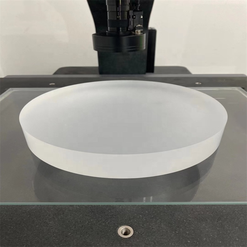
Custom Size Clear Fused Quartz Plate Premium Quality (1100C)
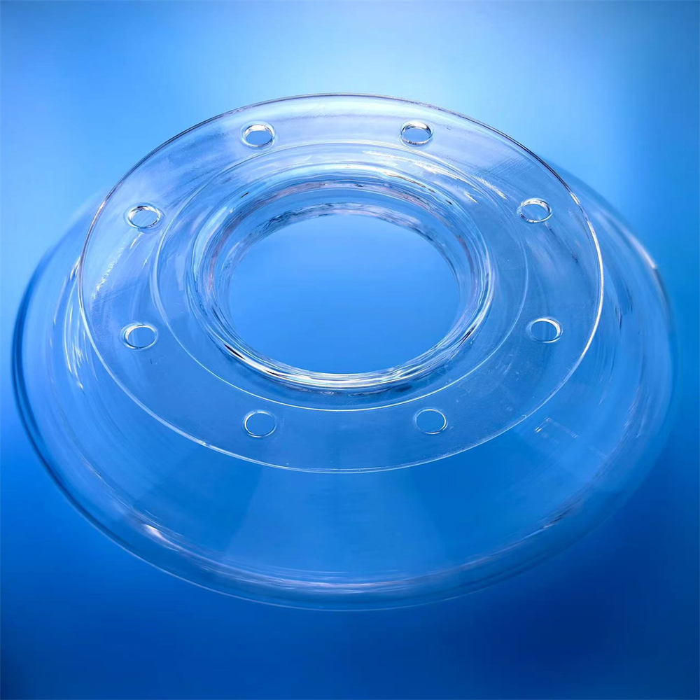
Custom High Purity Flange Twin Quartz Tube & Ring Assembly
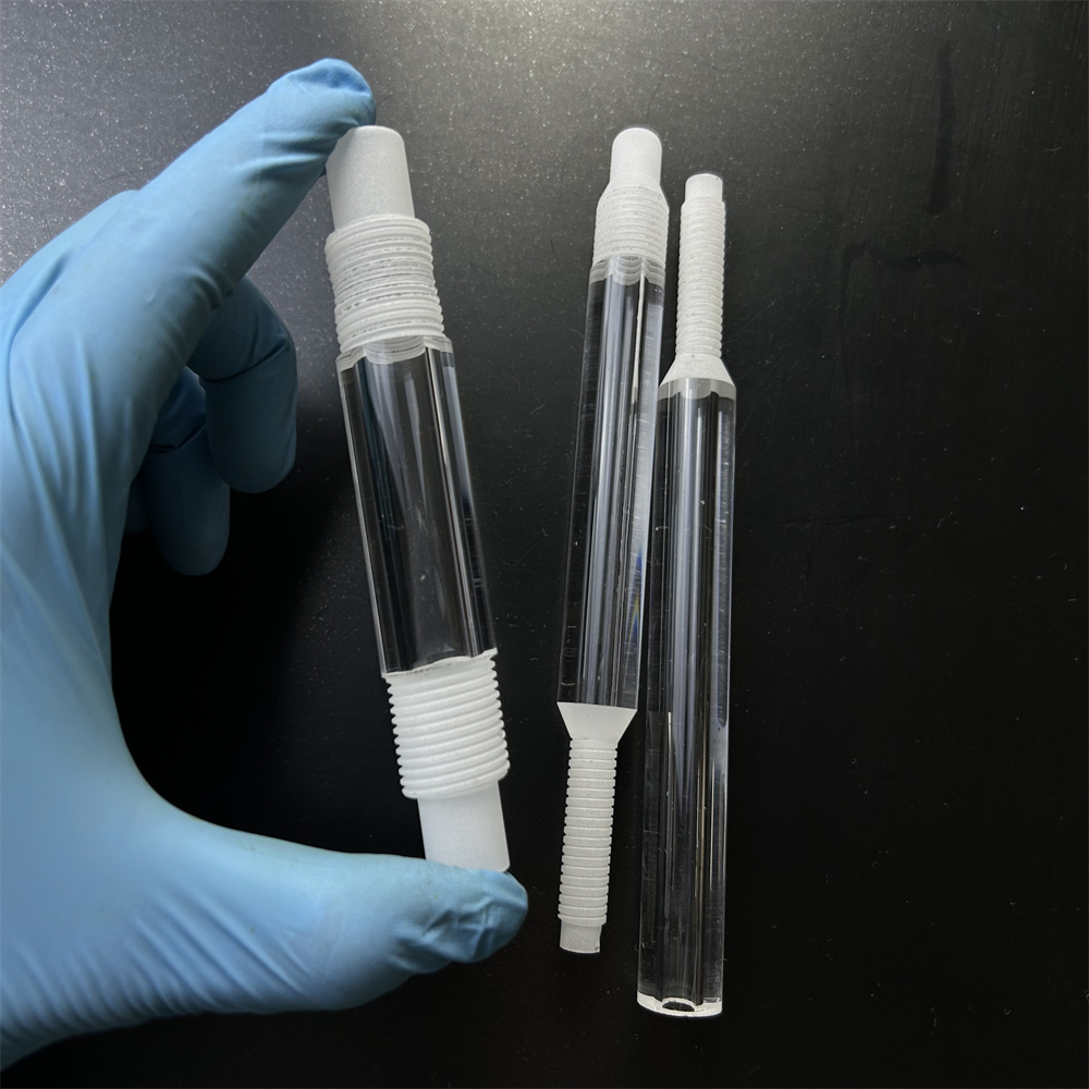
Customized High Purity Threaded UV Quartz Tube & Precision Collar
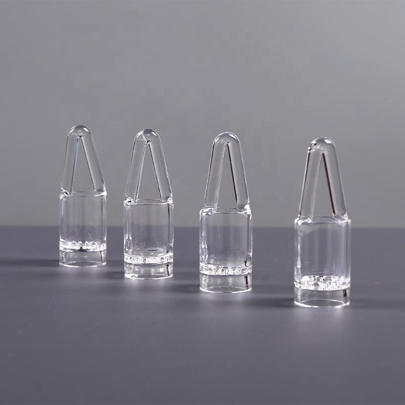
High Pressure 99.99% Pure Quartz Tube & Heavy Wall Flange Ring
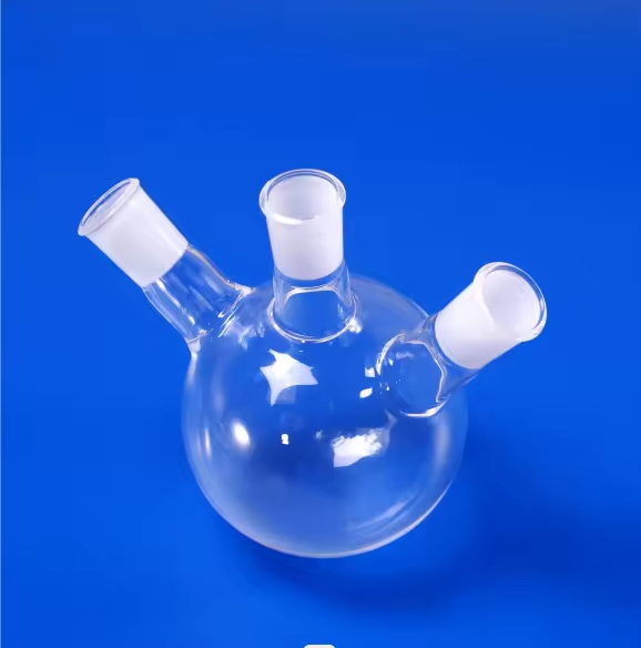
High Temperature Resistance Quartz Twin Tube Flask & Ring Seals
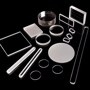
Optical Grade Fused Quartz Window & Wafer Support Discs
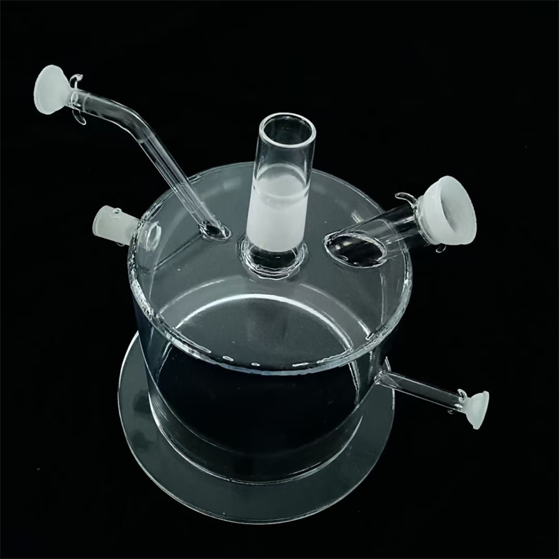
Customized High Pressure Clear Quartz Cylinder & Sealing Ring
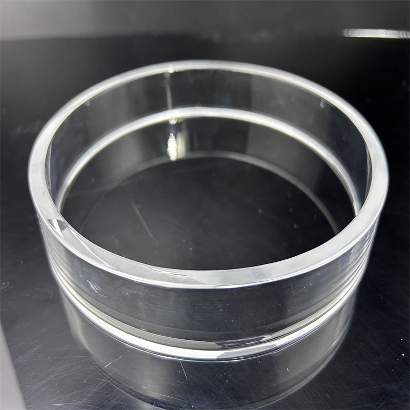
Corrosion-Resistant High Purity Fused Quartz Bell Jar & Ring Set
1. The Strategic Role of High-Purity Quartz Rings in Gwangju’s Semiconductor Ecosystem
As South Korea expands its high-tech sovereignty via the Gwangju Metropolitan Autonomous Region’s AI Semiconductor Hub and the Cheomdan L2 Industrial Complex, local fabrication plants (fabs), OSAT (Outsourced Semiconductor Assembly and Test) leaders like Amkor Technology Korea Gwangju, compound semiconductor research units at GIST (Gwangju Institute of Science and Technology), and photomask foundries require ultra-clean consumable components. Among these critical consumables, semiconductor quartz rings—including plasma focus rings, outer shield rings, gas injection rings, furnace flange rings, and retaining rings—play a vital role in maintaining process reproducibility, plasma stability, and wafer yield.
The manufacturing environment in Gwangju is evolving rapidly toward sub-5nm logic packaging, high-frequency GaN/SiC power electronics, and high-density memory modules. Processing these advanced devices involves aggressive fluorine-based dry plasma etching (e.g., CF4, C4F8, CHF3 gases combined with high RF bias power) and thermal CVD operations exceeding 1100°C. Under these severe conditions, standard borosilicate or low-grade silica rings suffer from micro-cracking, plasma erosion, devitrifcation, and heavy metallic particle shedding. Sourcing custom-machined, high-purity synthetic and flame-fused quartz rings directly from qualified factory partners ensures operational longevity, reduces chamber downtime, and lowers overall cost-per-wafer (CPW).
Information Gain Insight for Gwangju Process Engineers: Our custom-machined quartz focus rings are crafted using high-purity synthetic fused silica with hydroxyl (OH) content controlled below 5 ppm or targeted at 200 ppm depending on UV transmission versus thermal shock needs. This precise control limits plasma micro-trenching and particle contamination in inductively coupled plasma (ICP) etch chambers.
Precision Fabrication Capabilities for Semiconductor Quartz Rings
Advanced mechanical, laser, and thermal processing technologies designed to meet strict semiconductor OEM specifications.
5-Axis CNC Precision Machining
Equipped with ultrasonic-assisted high-speed CNC diamond grinders, our facilities achieve outer diameter tolerances of ±0.005mm and wall parallelism under 0.002mm on quartz focus and edge rings up to 450mm in diameter.
Laser Micro-Drilling & Grooving
Pico-second laser processing enables burr-free micro-hole arrays, retention notches, and thermal expansion slots without micro-fissures or stress concentrations that trigger ring fractures in vacuum plasma chambers.
Cleanroom Acid Washing & Fire Polishing
Every ring undergoes double-sided precision fire polishing, followed by Class 100 cleanroom HF/HNO3 acid etching to strip surface metallic ions (Fe, Cu, Na, K) and full vacuum baking to minimize outgassing.
2. Material Science Comparison: Selecting the Right Quartz Grade for Etch vs. Thermal Rings
Choosing the correct fused silica material grade is crucial when sourcing quartz rings for Gwangju’s semiconductor lines. Fabs often experience unexpected ring erosion or lattice thermal shock when substituting standard thermal quartz into fluorine plasma environments without adjusting material density and impurity levels.
| Quartz Material Grade | SiO2 Purity | OH Content | Typical Impurities (Fe, Na, K, Al) | Primary Application in Gwangju Fabs |
|---|---|---|---|---|
| Natural Flame-Fused Quartz (Electrically Fused) | ≥ 99.99% | < 5 ppm | Al: 8-15 ppm, Fe: < 0.2 ppm, Na: < 0.5 ppm | High-temperature LPCVD diffusion furnace rings, process tube sealing flanges (up to 1150°C). |
| High-Purity Synthetic Fused Silica | ≥ 99.999% | 10 - 200 ppm | Total Metals < 0.1 ppm (Near Zero Metallic Traps) | Extreme plasma etch focus rings (RIE/ICP), advanced EUV stepper lens rings, 3D NAND etch shields. |
| Ozone-Free Clear Quartz Glass | ≥ 99.99% | 15 - 30 ppm | Fe < 0.1 ppm, Titanium doped | UV curing rings, photolithography stepper alignment rings, photoresist strip chambers. |
| Opaque (Bubbled) Fused Quartz | ≥ 99.95% | < 10 ppm | Total Metals < 20 ppm | Thermal insulation barrier rings in rapid thermal processing (RTP) and epitaxy tool flanges. |
Plasma Erosion Mechanism in Fluorine Atmospheres
In dry etching tools (Lam Research, TEL, Applied Materials, or South Korean OEM platforms like Jusung Engineering and Wonik IPS), quartz focus rings surround the semiconductor wafer to homogenize RF plasma sheath potential across the wafer edge. When CF4/O2 or C4F8 plasma strikes the quartz ring, reaction products like SiF4 gas are generated. Over time, volatile silicon tetrafluoride formation thins the inner step of the focus ring, disrupting uniform edge yield.
By employing high-density, bubble-free synthetic silica with tight OH stoichiometry, our engineered quartz rings demonstrate a 18% to 27% reduction in plasma erosion velocity compared to standard commercially available quartz rings, directly extending PM (Preventive Maintenance) cycles from 250 RF hours to over 320 RF hours.
Localized Application Scenarios in Gwangju’s Tech Corridor
Custom quartz rings tailored for specific tool sets across Gwangju industrial zones.
1. Advanced OSAT & Chiplet Packaging (Cheomdan L2 District)
Gwangju’s advanced packaging ecosystem utilizes custom quartz carrier rings and substrate support rings during fan-out panel-level packaging (FOPLP) and TSV (Through-Silicon Via) processing. High surface flatness (< 0.003mm TIR) prevents wafer bowing and thermal displacement during high-temperature polymer curing.
2. Compound Semiconductor (GaN/SiC) Fabs & GIST R&D
For high-power wide-bandgap device epitaxy, specialized quartz gas distribution rings and bell-jar sealing collars provide vacuum integrity at temperatures exceeding 1200°C without leeching trace iron or alkali metals into the crystal lattice.
3. Dry Plasma Etching Chambers (Focus & Edge Rings)
Custom direct-replacement focus rings compatible with 200mm and 300mm wafer etch chambers. Our CNC chamfering and diamond edge polishing prevent particle flaking, reducing edge-exclusion zones on silicon wafers.
4. LPCVD & PECVD Thermal Furnace Tube Flanges
Heavy-duty, thick-wall flanged quartz rings designed to seal oxidation, diffusion, and LPCVD vertical tube furnaces. High thermal shock resistance enables rapid ramp rates without risk of cataclysmic ring cracking.
3. Localized Sourcing Trends & Supply Chain Dynamics in Gwangju
Historically, semiconductor fabs in Gwangju relied on long supply chains via secondary distributors or Japanese original equipment manufacturers (OEMs), resulting in 12-to-16-week lead times and high markups for consumable quartz parts. Today, procurement directors in South Korea are pursuing direct factory sourcing models to establish resilient, cost-optimized supply networks.
Key Sourcing Drivers for Gwangju Procurement Managers:
- Cost Reduction Mandates: Direct manufacturing partnerships with premier quartz specialists eliminate intermediary surcharges, delivering 30% to 45% cost savings on recurring focus ring orders.
- Custom CAD/Drawing-to-Part Capability: Ability to manufacture directly from customer STEP/DWG files or reverse-engineer legacy chamber rings with exact dimensional alignment.
- Rapid Expedited Delivery: Prototyping in 7-10 business days with direct air shipping into Incheon International Airport or Muan International Airport, bringing total lead times down to under 3 weeks.
- Small-Batch & 1-Piece MOQ Support: Facilitating immediate R&D trials for modified focus ring geometries without enforcing high minimum order volumes.
Enterprise Advantages: Direct Factory Manufacturing & Supply
Headquartered near Donghai County—the crystal capital of China—Lianyungang Zelvo Quartz Products Co., Ltd. brings full end-to-end quartz manufacturing control to global buyers.
99.999% Purity Guaranteed
We source raw quartz sand directly from high-purity crystalline deposits, applying triple acid purification. Every batch is certified with spectrographic chemical analysis to verify trace metal levels before processing.
Full In-House Fabrication Suite
From initial glass tube extrusion and quartz block cutting to 5-axis ultrasonic CNC grinding, laser drilling, slotting, and flame welding—100% of production remains under our strict quality control.
Reliable Global Logistics to Korea
Custom shock-resistant wooden crates with vacuum sealed cleanroom packaging ensure your precision quartz rings arrive at your Gwangju plant with zero micro-fractures, surface contamination, or dimensional distortion.
Frequently Asked Questions by Gwangju Procurement & Process Engineers
Clear answers addressing technical specifications, lead times, quality assurance, and order logistics.
What drawing formats do you require for custom quartz focus ring quotes?
We accept standard 2D and 3D CAD files including STEP, IGES, DWG, DXF, and PDF. Our engineering team conducts a complimentary Design for Manufacturability (DFM) review within 2 hours of receipt, confirming wall thickness feasibility, chamfer radius tolerances, and edge polish needs.
How do your quartz rings handle harsh fluorine (CF4/SF6) plasma environments?
Our synthetic fused silica rings feature high atomic stoichiometry and near-zero micro-porosity. This minimizes plasma micro-sputtering, preventing surface roughening and particle detachment during deep silicon reactive ion etching (RIE) cycles in semiconductor chambers.
What is the typical shipping lead time from your factory to Gwangju, South Korea?
Standard prototyping orders take 7 to 10 business days for CNC machining and cleanroom acid polishing. Air express shipping via DHL/FedEx or direct air cargo to Incheon/Muan takes 2 to 3 days, making total door-to-door delivery within 2 to 3 weeks.
Can you supply certified low-alkali quartz rings for mobile or automotive IC lines?
Yes. We provide full spectrographic material certificates verifying total metallic impurities (Na, K, Li, Fe, Cu) below 5 ppm, with specialized optical/synthetic grades reaching under 0.1 ppm total metals for sensitive mobile logic and automotive power IC manufacturing.
What is your Minimum Order Quantity (MOQ) for custom quartz parts?
Our MOQ is 1 piece for standard custom drawings. We actively support R&D engineering trials, chamber retrofits, and university lab testing (e.g., GIST research projects) prior to mass production volume scaling.
Accelerate Your Gwangju Fab Sourcing with Direct OEM Quartz Rings
Send us your CAD drawings or dimensional specifications today. Our engineering sales team will provide a technical DFM review and competitive factory-direct quote within 2 hours.