Featured Semiconductor Quartz Components
Synthesized from high-purity natural silica in Donghai and processed via multi-axis CNC micro-machining, laser profiling, and flame polishing for immediate cleanroom deployment.
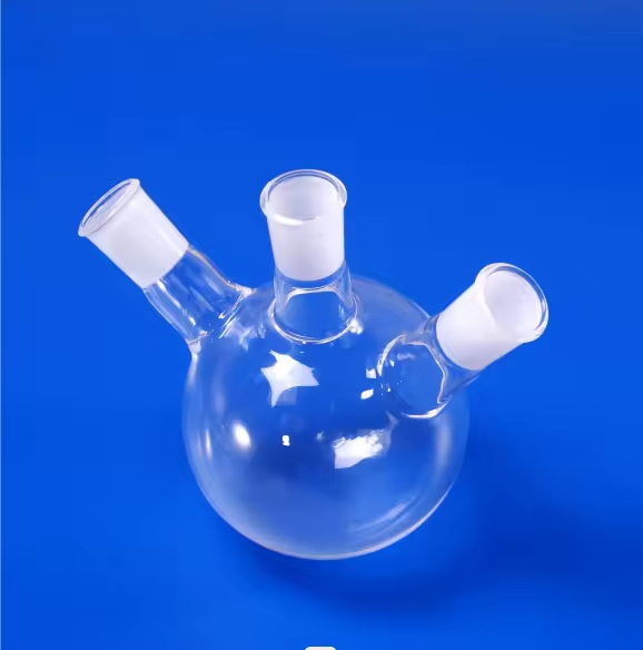
High Temperature Resistance Transparent Quartz Glass Twin Tube Bottom Flask
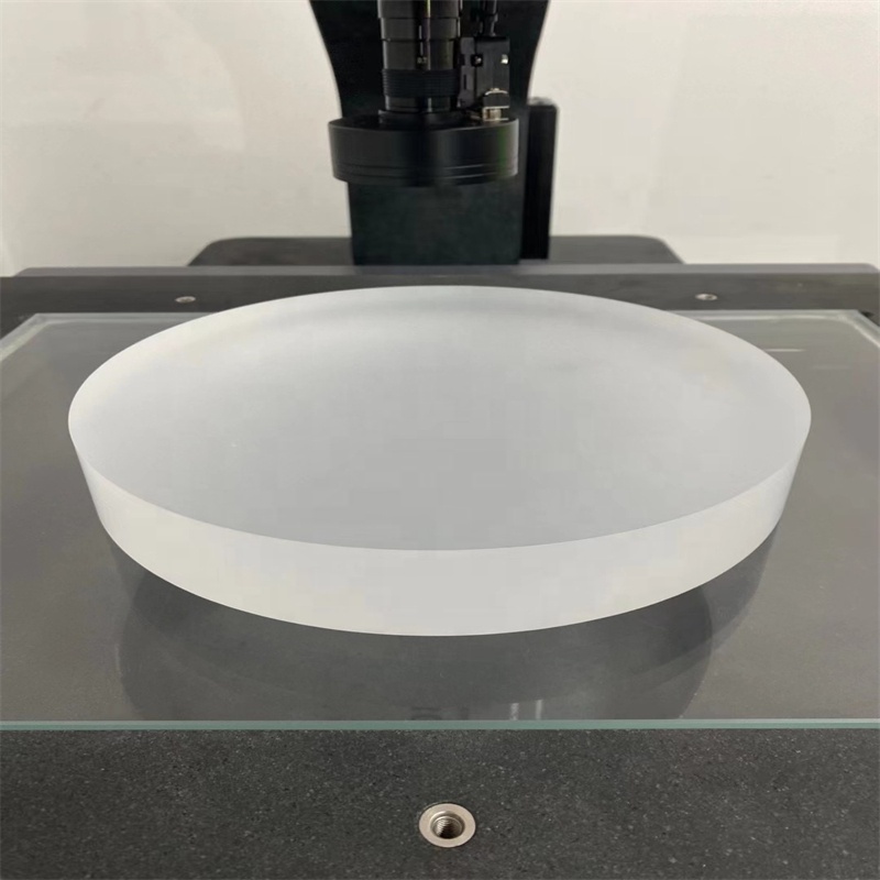
Custom Size Clear Fused Quartz Plate Premium Quality High Temp (1100°C)
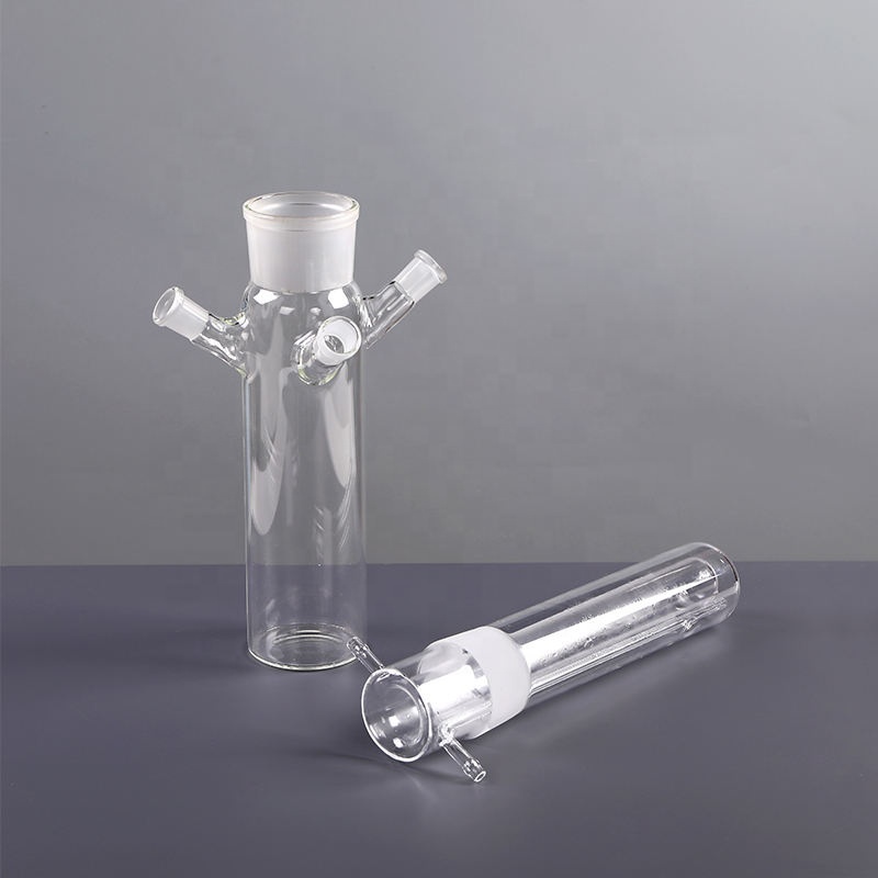
Customized High-Purity Quartz Glass Reactor Container
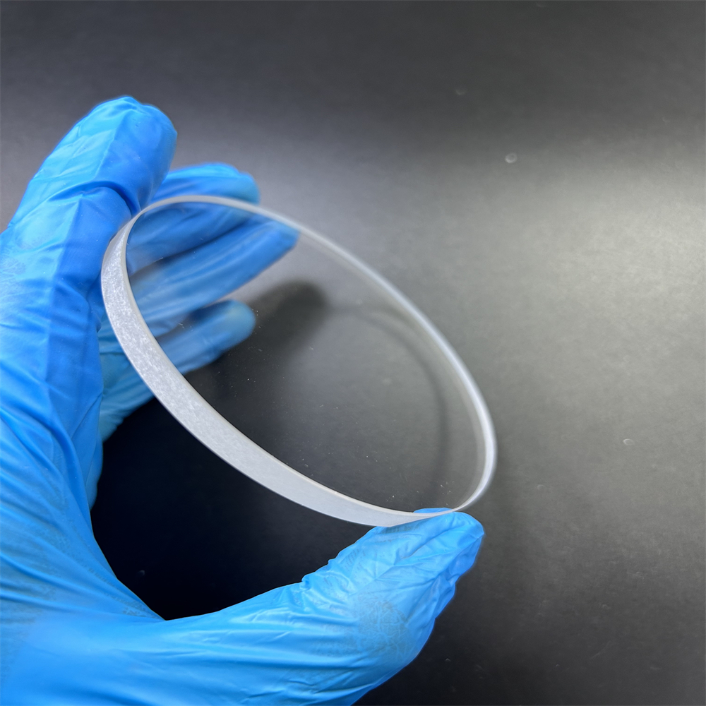
High Pressure Fused Silica Quartz Glass Wafer Transparent UV Sheet
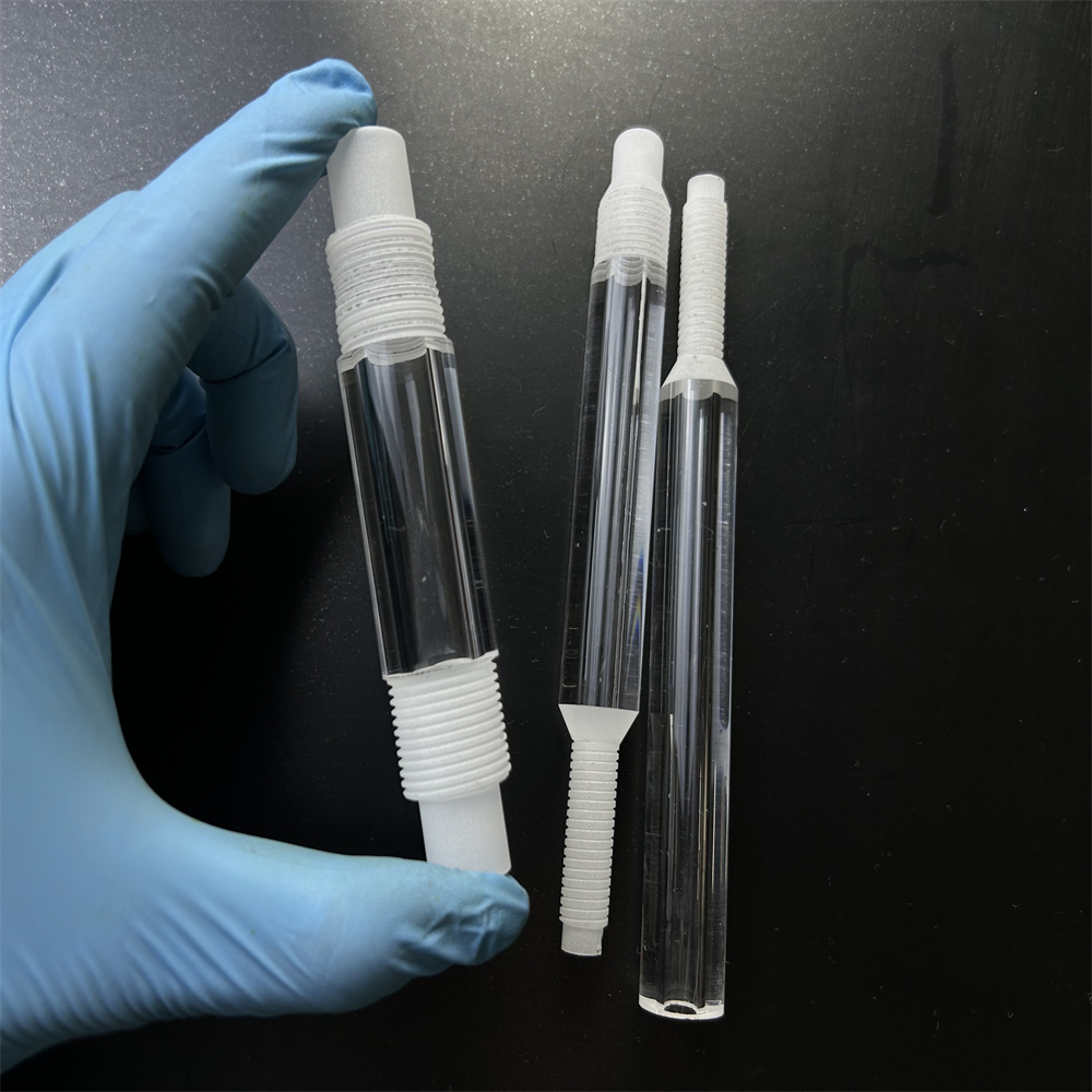
Customized High Purity Threaded Transparent UV Quartz Glass Tube
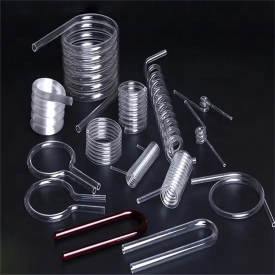
Custom Different Sizes U-Bent Quartz Glass Spiral Tube
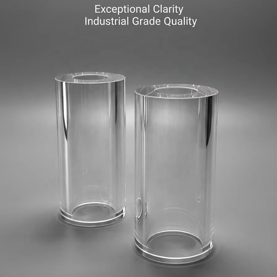
Factory Custom Both Ends Polished High Purity Quartz Twin Tube
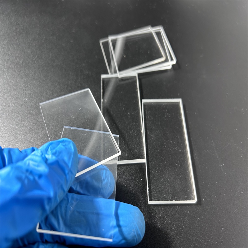
Customized High Temperature Transparent Fused Quartz Glass Sheet
Precision Semiconductor Quartz Rings: Material Science, Etch Kinetics, and Thermal Equilibrium
In modern microelectronics fabrication, reactive ion etching (RIE), inductively coupled plasma (ICP) etching, chemical vapor deposition (CVD), and rapid thermal processing (RTP) operate under severe thermo-chemical and plasma stress. As wafer nodes compress toward deep sub-micron dimensions and wide-bandgap semiconductors (such as Silicon Carbide [SiC] and Gallium Nitride [GaN]) become mainstream across European automotive and power electronic roadmaps, the mechanical reliability and purity of chamber consumables dictate production yields. Among these chamber components, the semiconductor quartz ring—serving variously as a focus ring, shadow ring, edge ring, clamp ring, or gas containment collar—serves as the critical consumable barrier safeguarding the wafer boundary.
Manufactured by Lianyungang Zelvo Quartz Products Co., Ltd. within Donghai County—China's internationally recognized crystal capital—our semiconductor-grade fused quartz rings utilize synthetically fused and high-purity electro-fused silica feedstocks. Achieving a Silicon Dioxide (SiO&sub2;) purity exceeding 99.99% to 99.999%, these rings exhibit virtually zero lattice defects, negligible bubble inclusion densities, and extremely stringent alkali metal restrictions (Sodium, Potassium, Lithium combined < 1.0 ppm). This chemical neutrality prevents parasitic mobile ion contamination that causes gate oxide breakdown in sub-micron MOS gates and power transistor junctions.
Taxonomy of Semiconductor Quartz Rings: Functional Classifications
Different process chambers impose unique degradation mechanisms on quartz rings. We categorize and fabricate custom quartz rings matched specifically to the kinetic conditions inside leading dry etch, epitaxial, and diffusion equipment:
Plasma Etch Focus Rings
Surrounds the electrostatic chuck (ESC) to guide CF&sub4;, C&sub4;F&sub8;, and SF&sub6; fluorocarbon plasma ions uniformly to the wafer edge, preventing premature plasma collapse and perimeter arcing.
RTP & Oxidation Slip Rings
Engineered for rapid thermal annealing (up to 1250°C) with low coefficient of thermal expansion (5.5 × 10&supmin;&sup7;/K) to equalize radial thermal gradients and prevent wafer crystal slip dislocations.
LPCVD / PECVD Clamp Rings
Secures wafers mechanically against heating chucks during dielectric or polysilicon film deposition, featuring high chemical resistance against silane, ammonia, and NF&sub3; in-situ chamber cleans.
Chamber Gas Distribution Rings
High-aspect-ratio perforated annular quartz manifolds featuring micron-precision laser-drilled orifices to deliver uniform precursor gas flow dynamics across 100mm, 150mm, and 200mm process substrates.
Material Purity & Thermomechanical Metrics (ICP-MS Validated)
Cleanroom engineers across European foundries require full trace element disclosure. Trace elements such as Fe, Cu, and Ni serve as deep-level recombination centers that deteriorate minority carrier lifetimes, while volatile alkalis (Li, Na, K) trigger threshold voltage drifts. Below is the reference operational and impurity analysis matrix for our semiconductor quartz rings:
| Property / Elemental Constituent | Testing Method / Unit | Zelvo Standard Grade (99.99%) | Zelvo Semi-Ultra Grade (99.999%) |
|---|---|---|---|
| Silicon Dioxide (SiO&sub2;) Content | Gravimetric / Difference | ≥ 99.99% | ≥ 99.999% |
| Density (ρ) | Archimedes Principle (g/cm³) | 2.20 | 2.201 |
| Continuous Working Temperature | Pyrometric Analysis (°C) | 1100 °C | 1150 °C |
| Softening Point / Annealing Point | Dilatometer (°C) | 1683 °C / 1215 °C | 1710 °C / 1230 °C |
| Thermal Expansion Coeff. (20°C–320°C) | Dilatometry (K&supmin;¹) | 5.5 × 10&supmin;&sup7; | 5.4 × 10&supmin;&sup7; |
| Dielectric Strength (20°C) | Short-time breakdown (kV/mm) | 25 – 40 | 35 – 50 |
| Aluminum (Al) Content | ICP-MS (ppm) | ≤ 14.0 | ≤ 4.0 |
| Iron (Fe) Content | ICP-MS (ppm) | ≤ 0.2 | ≤ 0.05 |
| Sodium (Na) / Potassium (K) | ICP-MS (ppm) | ≤ 0.7 / ≤ 0.5 | ≤ 0.1 / ≤ 0.1 |
| Copper (Cu) / Nickel (Ni) | ICP-MS (ppm) | ≤ 0.05 / ≤ 0.05 | ≤ 0.01 / ≤ 0.01 |
| Hydroxyl (OH&supmin;) Radical Content | FTIR Spectroscopy (ppm) | < 20 (Flame Fused) | < 5 (Vacuum Electro-fused) |
Localized Semiconductor & Nanotechnology Applications Across Portugal
Portugal's high-tech landscape is undergoing rapid modernization, anchoring critical nodes of the European microelectronics value chain. Our engineered quartz rings, plates, and process components are explicitly customized to fulfill the demanding prototyping and manufacturing requirements of Portuguese institutions and industrial players:
Integration with Portugal's Premier Research & Industrial Clusters
From the Minho innovation corridor down to the Greater Lisbon area, Portuguese cleanrooms leverage custom fused silica for rigorous micro-fabrication, advanced sensor production, and photonics R&D:
INL & Minho Nanotech Hub (Braga)
At the International Iberian Nanotechnology Laboratory (INL) in Braga, advanced cleanrooms execute 200mm lithography, 2D material synthesis, spintronics, and quantum device prototyping. Our custom plasma etch rings and high-transmittance optical silica wafers provide the sub-micron physical tolerance (±0.01 mm) essential for non-standard exploratory substrates and cryogenic RF setups.
Automotive Microelectronics (Braga & Porto)
With industrial powerhouses like Bosch Car Multimedia Portugal operating massive electronics centers in Braga, alongside automotive tier-suppliers across Northern Portugal, demand for high-reliability sensor packaging and high-temperature power electronics (SiC/GaN) is surging. Our quartz diffusion tubes, quartz boats, and thermal focus rings ensure zero sodium drift during high-temperature gate oxidation and diffusion cycling.
Taguspark & Lisbon Microelectronics (Oeiras)
Taguspark in Oeiras and the research labs associated with Instituto Superior Técnico (IST) and Instituto de Telecomunicações (IT) lead Portuguese integrated circuit design and photonics packaging. Our laser-machined optical quartz sheets, custom twin tubes, and UV quartz inspection windows support photonic integrated circuit (PIC) validation and high-vacuum sputtering test benches.
Portugal's Semiconductor Trajectory & European Chips Act Alignment (2025–2030)
The European Union's ambitious objective under the European Chips Act—to secure 20% of global semiconductor production by 2030—has triggered significant downstream investments across Southern Europe. In Portugal, this momentum manifests through the Plano Nacional para os Semicondutores, direct European Regional Development Funds (ERDF), and Horizon Europe partnerships focusing on automotive sensor assembly, micro-electromechanical systems (MEMS), and compound semiconductor packaging.
Historically reliant on third-party broker networks in Central Europe, Portuguese labs and foundries frequently experienced exorbitant lead times (16 to 26 weeks) and inflated pricing for replacement quartz chamber components. Zelvo Quartz fundamentally solves this supply chain vulnerability. By maintaining direct drawing-to-fabrication agility in Donghai and facilitating expedited air freight into Humberto Delgado Airport (LIS) and Francisco Sá Carneiro Airport (OPO), Portuguese cleanroom managers acquire precision OEM-equivalent or custom-engineered quartz focus rings in 2 to 4 weeks, with full material batch trace analysis.
Furthermore, as Portuguese facilities advance sustainable semiconductor manufacturing initiatives, the exceptional thermal longevity and clean re-workability of our fused quartz components substantially reduce annual consumable waste. Because our vacuum electro-fused silica features low initial hydroxyl content (OH&supmin; < 5 ppm), our rings resist rapid devitrification (cristobalite crystal growth) at elevated temperatures, doubling the mean time between replacement (MTBR) during heavy dry-etch fluorine cycles.
Engineering Advantages: Why Cleanrooms Rely on Zelvo Quartz
Lianyungang Zelvo Quartz Products Co., Ltd. merges the raw mineral superiority of Donghai County with precision German-style optical machining. We offer engineering teams in Portugal distinctive operational advantages:
100% Onsite-Verified Purity
Our raw quartz sand is chemically refined and vacuum-fused to ensure ≥99.99% SiO&sub2;. Every semiconductor ring batch is verified via inductively coupled plasma mass spectrometry (ICP-MS) to guarantee zero contamination of customer chambers.
Micron-Level CNC & Laser Machining
We deploy 5-axis CNC ultrasonic machine centers, precision coordinate grinding, and high-speed CO&sub2; laser drilling to fabricate annular steps, internal grooves, bevels, and micro-holes with dimensional limits within ±0.01 mm.
Agile Prototyping ≤2h Feedback
We support a strict 1-piece Minimum Order Quantity (MOQ). Cleanroom researchers can send 2D/3D CAD drawings (STEP, DXF, DWG) and receive structural feasibility reviews and formal pricing within 2 hours on working days.
Cleanroom Ultrasonic Decontamination
Prior to packaging, quartz rings undergo acid etching (HF/HNO&sub3; neutralization) to strip micro-particulates, followed by 18.2 MΩ·cm deionized water multi-stage ultrasonic scrubbing and vacuum poly-sealing for direct cleanroom transfer.
Safe European Logistics & DDP Terms
Suspension foam encasement and reinforced wooden crating eliminate mechanical shock damage during transit. We manage seamless Incoterms (DDP, DAP, CIP) directly to Porto, Braga, Coimbra, Aveiro, and Lisbon without customs hassle.
10+ Years Dedicated Glassworking Pedigree
Our workshop team leverages master flameworking expertise combined with modern interferometric quality control, ensuring zero internal stress birefringence and complete geometric fidelity to your blueprints.