Featured Custom Fused Silica & Quartz Components
Engineered for High-Pressure Chambers, UV Photolithography, Laser Systems, and Semiconductor Processing
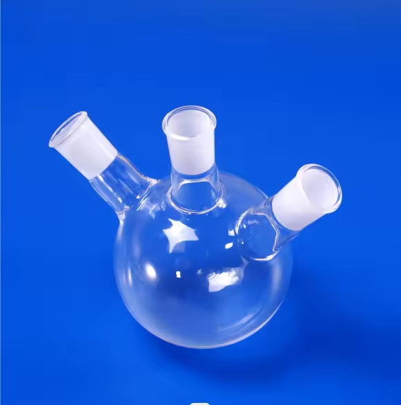
High Temperature Resistance Transparent Quartz Glass Twin Tube Bottom Flask
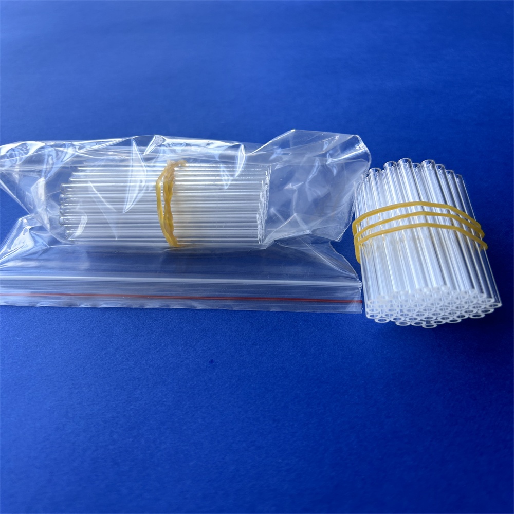
Small Diameter 0.1-20mm High Temperature Resistant 99.99% Pure Quartz Capillary Tube
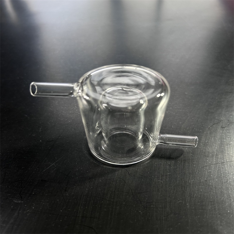
Custom 99.99% Pure Ozone Free Quartz Glass Reactor Twin Tube Services
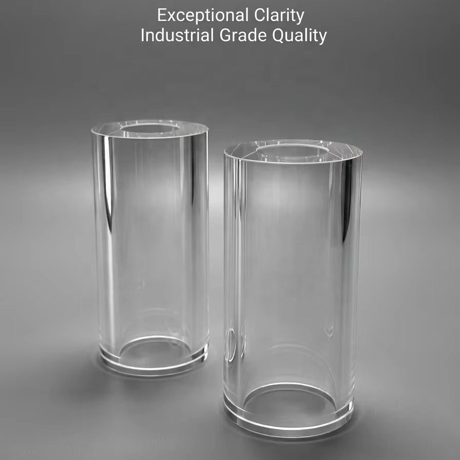
Factory Custom Both Ends Polished High Purity Transparent Quartz Twin Tube
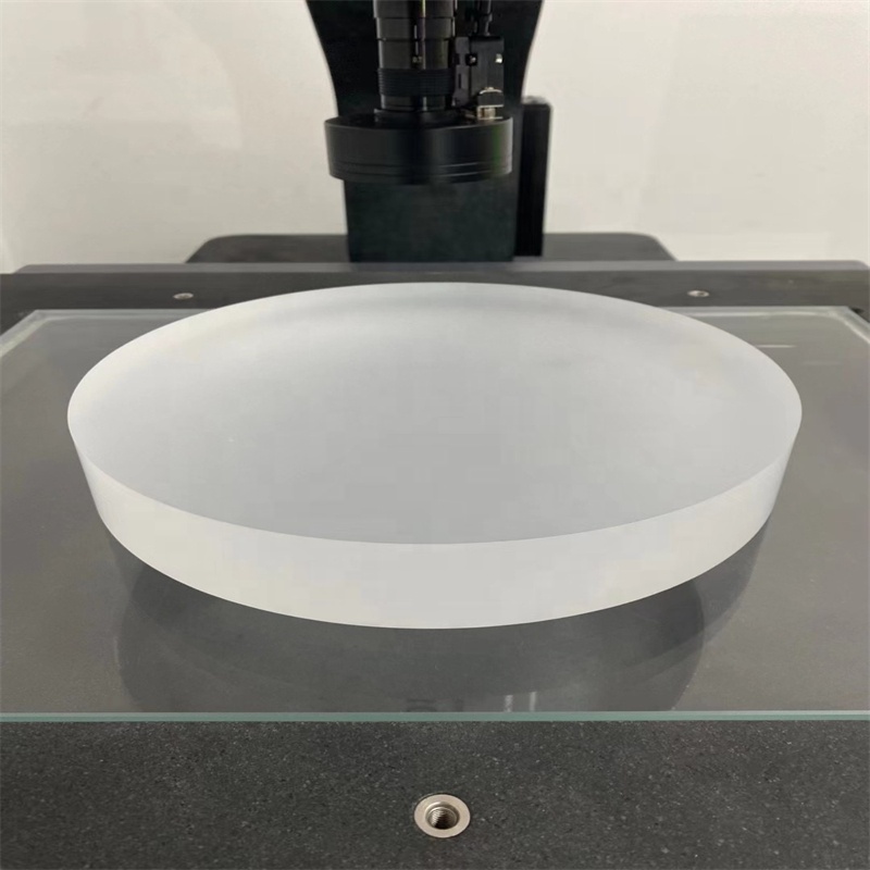
Custom Size Clear Fused Quartz Plate Premium High Temperature Resistance Glass Sheet
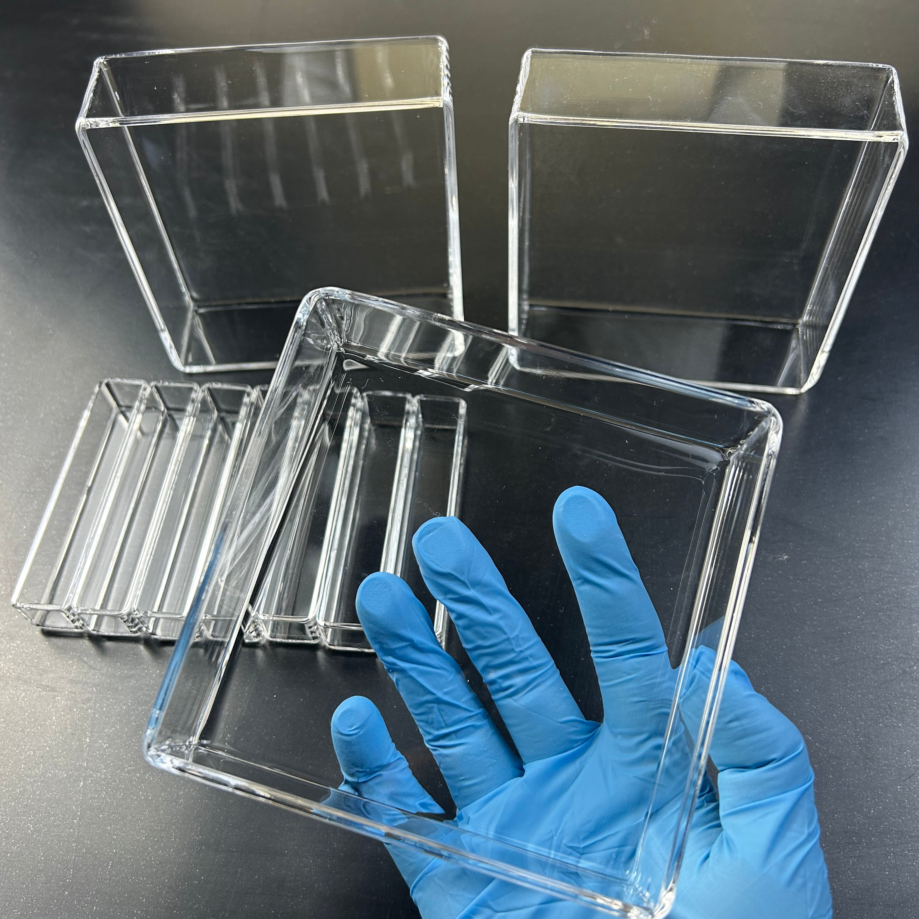
Customized Fused Quartz Glass High Temperature Circular Cylinder Crucible Tank
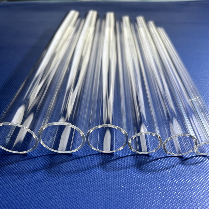
Transparent High Pressure 99.99% Pure Quartz Glass Tube for Boiler & Furnace
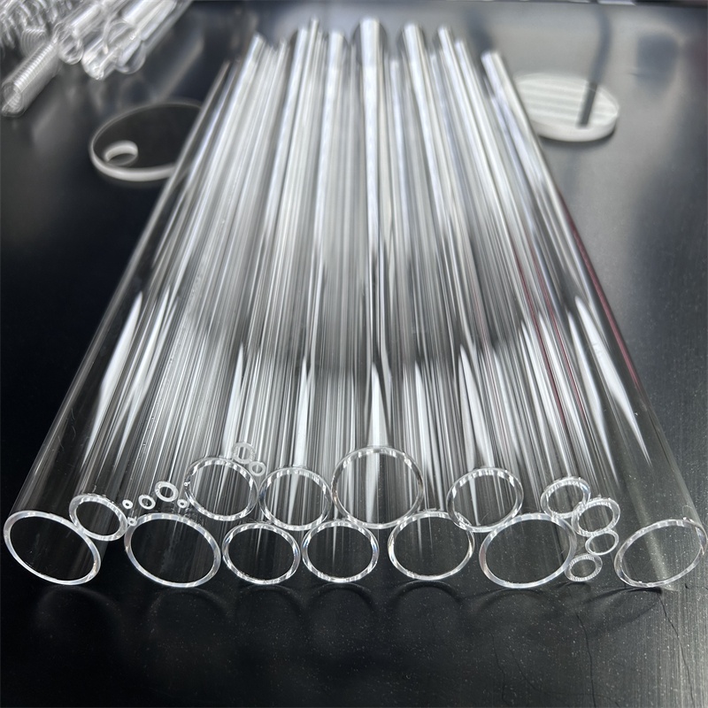
High Temperature Clear 99.99% Pure Fused Quartz Twin Tube with Bending Services
Technical Whitepaper: Precision Fused Silica Optical Windows Engineering Framework
In modern optoelectronic, semiconductor wafer fabrication, and high-energy laser systems, selecting the appropriate optical substrate is paramount. Custom OEM fused silica windows serve as critical isolation barriers, viewport windows, and optical flat substrates designed to operate seamlessly under harsh conditions, extreme thermal cycling, and high radiation fluences. Unlike standard soda-lime or borosilicate glass, fused silica (Silicon Dioxide, SiO₂) offers unmatched physical purity, exceptional UV-to-NIR spectral transmission, near-zero thermal expansion, and outstanding resistance to thermal shock.
Precision manufacturing of custom fused silica windows requires strict controls over raw material synthesis, precision optical polishing, sub-aperture CNC machining, and state-of-the-art metrology. Factories specializing in high-grade fused silica components utilize specialized synthetic precursors (such as SiCl₄ oxidation) to achieve chemical purity exceeding 99.999%, virtually eliminating metallic impurities (Fe, Cu, Ti) that cause micro-absorption and optical distortion in high-power laser applications.
Synthetic vs. Natural Fused Silica Material Grades
| Standard Grade Code | Material Origin | Spectral Range | Hydroxyl (OH⁻) Content | Primary Target Application |
|---|---|---|---|---|
| JGS1 (UV Synthetic Fused Silica) | Synthetic SiCl₄ Reaction | 185 nm – 2500 nm (Deep UV) | High OH⁻ (800 – 1200 ppm) | Excimer lasers, DUV photolithography, UV optics, fluorescence viewport windows. |
| JGS2 (Optical Fused Quartz) | High-Purity Natural Quartz Crystal | 220 nm – 2700 nm (UV-Vis-NIR) | Medium OH⁻ (150 – 300 ppm) | High-temperature viewports, furnace sight glasses, optical flats, observation windows. |
| JGS3 (Infrared Synthetic Silica) | Vapor Phase Axial Deposition | 260 nm – 3500 nm (Near to Mid IR) | Low OH⁻ (< 5 ppm) | Infrared spectroscopy, CO2 laser optics, laser sensor windows, high-IR transmittance optics. |
When specifying OEM fused silica windows, optical design engineers must carefully weigh transmission efficiency against operating environmental stress. For example, in Deep Ultraviolet (DUV) applications operating at 193nm (ArF excimer wavelength) or 248nm (KrF excimer wavelength), the absorption induced by trace hydroxyl impurities can severely degrade systemic efficiency. Synthetic JGS1 silica minimizes solarization and phase shifts, delivering light transmission exceeding 92% (uncoated) down to 185nm. Conversely, for near-infrared (NIR) and thermal sensing platforms, JGS3 eliminates the dominant absorption band around 2.73 µm caused by OH⁻ stretching vibrations, guaranteeing crystal-clear thermal imaging and laser throughput.
Enterprise Advantages & Factory Capabilities
Lianyungang Zelvo Quartz Products Co., Ltd. – Strategic Manufacturing Partner in China's Crystal Capital
Geographic Raw Material Hub
Situated in Donghai County, Jiangsu Province—globally recognized as China’s "Crystal Capital"—Zelvo Quartz leverages direct integration with premier raw-material supply chains. This regional synergy guarantees uninterrupted access to 99.99% high-purity silica sand, lowering raw procurement overhead while ensuring batch-to-batch chemical stability.
Ultra-Precision Fabrication
Equipped with 5-axis CNC ultrasonic glass machining centers, double-sided optical planetary lapping units, and multi-axis laser drilling rigs. We maintain strict geometric tolerances: surface flatness up to λ/10 per 25mm, surface scratch-dig quality of 20-10 or 10-5 MIL-PRF-13830B, and parallelism under 5 arcseconds.
100% Quality Verification
Every custom fused silica window and component undergoes stringent quality assurance. Our internal inspection laboratory features ZYGO laser interferometers, UV-Vis-NIR spectrophotometers, and 3D coordinate measuring machines (CMM) to verify surface roughness (Ra < 0.5nm), optical transmission, and dimensional fidelity before dispatch.
Tailored Drawing-Based OEM Manufacturing
At Zelvo Quartz, we recognize that off-the-shelf optical components rarely satisfy complex experimental or industrial requirements. Whether you require micro-sized quartz capillary windows (0.1mm diameter), multi-step flanged furnace viewports, custom U-bent heating tubes, or large-format circular optical disks up to 800mm in diameter, our engineering team transitions your 2D/3D CAD drawings into production in record time.
With an agile manufacturing workflow, we welcome prototype orders starting from 1 Piece (MOQ = 1). Our technical account engineers provide rapid design-for-manufacturability (DFM) feedback within 2 hours, assessing thermal stress profiles, bevel specifications, and optimized coating strategies to minimize unit costs without compromising optical performance.
Manufacturing Specifications at a Glance
- Dimensional Tolerances: Up to ±0.01 mm for precision optics.
- Surface Roughness (Ra): Polished down to < 0.2 nm (Superpolished grade).
- Scratch-Dig Specs: 10-5, 20-10, 40-20, or 60-40 dependent on system sensitivity.
- Optical Flatness: λ/2, λ/4, or λ/10 @ 632.8 nm laser wavelength.
- Parallelism: < 10 arcseconds to eliminate optical beam steering.
- Custom Edge Treatments: Ground, chamfered, fire-polished, or step-grooved edges.
- Thin Film Coating Options: Anti-Reflective (AR), High-Reflective (HR), & Beamsplitter coatings.
Technological & Development Trends in Fused Silica Optics
Anticipating Next-Generation Demands across Semiconductor, Photonics, and Clean Energy Industries
1. Extreme Surface Superpolishing for High-Energy Lasers
As kilowatt and megawatt-class fiber lasers, ultrafast picosecond/femtosecond lasers, and fusion research platforms expand, standard optical polishing is no longer sufficient. Sub-surface damage (SSD) caused by micro-abrasives creates localized absorption centers that lower the Laser Damage Threshold (LDT). The trend in fused silica window manufacturing is shifting toward chemical-mechanical polishing (CMP) and ion beam machining (IBM) to achieve sub-angstrom surface roughness (Ra < 0.1nm), elevating laser power withstand capabilities beyond 20 J/cm² @ 1064nm (10ns pulse).
2. Deep-UV & Solarization Resistance for Semiconductor ALD/CVD
Sub-3nm chip production utilizes intense DUV and EUV illumination alongside harsh Atomic Layer Deposition (ALD) chemistry. Fused silica window viewports inside plasma chambers face continuous bombardment from reactive fluorine/chlorine gases and ionizing UV radiation. Modern quartz synthesis focuses on stabilizing hydrogen molecule concentrations inside the silica matrix to inhibit color-center formation (E' centers), preventing solarization and transmittance decay over thousands of operational hours.
3. Ultra-Thin & Large-Format Hermetic Glass Assemblies
Aerospace, defense sensor pods, and quantum computing chambers require ultra-thin fused silica optical wafers (thickness < 0.5mm) that can endure extreme pressure differentials. Simultaneously, astronomy and aerospace viewports demand monolithic synthetic quartz plates exceeding 500mm to 1000mm in clear aperture. Vacuum sealing these windows directly to dissimilar metals (such as Titanium, Kovar, or Stainless Steel) via active metal brazing or glass-to-metal hermetic bonding represents a crucial technological milestone.
4. Advanced Anti-Reflective (AR) & Hydrophobic Nano-Coatings
Uncoated fused silica reflects roughly 3.5% to 4% per surface due to Fresnel reflection. Modern OEM windows increasingly specify dual-band or broadband AR thin-film coatings deposited via Electron-Beam or Ion Assisted Deposition (IAD) technology. Incorporating outer hydrophobic and oleophobic nano-layers protects high-precision optics from oil condensation, water spots, and dust adhesion in outdoor military sight systems, marine LiDAR sensors, and industrial processing lines.
Future Procurement Trends for Global B2B Optical Buyers (2025–2030)
Global strategic sourcing for custom optical components has evolved dramatically. Industrial buyers, original equipment manufacturers (OEMs), and university research institutes are shifting away from traditional catalogue distributors in favor of direct factory partnerships. By interfacing directly with verified fused silica window factories, procurement officers eliminate distributor markups—often cutting component acquisition costs by 30% to 50% while securing direct engineering oversight.
Key procurement dynamics defining the next decade include:
- Agile Prototyping-to-Mass-Production Bridges: Buyers require seamless scaling from 1-piece R&D validation prototypes straight into thousands of batch units without renegotiating quality terms or undergoing multi-vendor requalification.
- Digital Quality Traceability: Modern B2B optical procurement contracts demand fully documented spectrophotometric transmission curves, material purity certifications (RoHS, REACH compliance), and interferometric surface contour maps delivered alongside shipping lots.
- Supply Chain Resilience & Lead-Time Compression: Relying on centralized manufacturing hubs like Donghai, China, enables automated raw material sourcing, drastically shortening production cycles for custom-machined quartz plates from months to 2–3 weeks.
- DDP (Delivered Duty Paid) Transparency: Overseas buyers prefer comprehensive export logistics where custom clearing, shock-resistant wooden crate packaging, and doorstep insurance are handled directly by the exporter under door-to-door delivery terms.
Frequently Asked Questions (FAQ)
Technical & Sourcing Answers for Precision Fused Silica Windows & Custom Quartz Optics
What purity levels are available for your fused silica windows and custom quartz plates?
What operating temperatures can custom fused silica windows withstand?
What surface quality and flatness specifications can your factory achieve for custom optical windows?
Can you manufacture custom quartz parts and windows directly from technical drawings?
What is your Minimum Order Quantity (MOQ) and sample lead time?
How do you protect fragile fused silica windows during international shipping?
Request Your Custom Fused Silica Window Quote Today
Send us your dimensions, drawing files, or material specifications. Our senior optics engineers will review your design and provide a competitive factory-direct quote with DFM feedback within 2 hours.