High-Purity Quartz Glass & Wafer Substrates
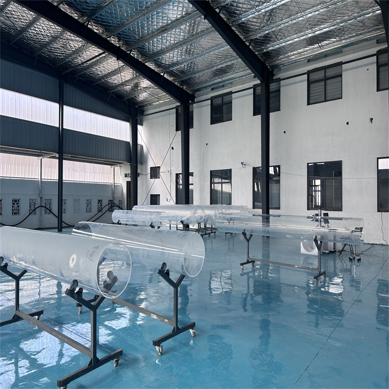
Manufactured under strict ISO 9001 standards from 99.99% SiO₂ fused silica. Our Donghai fabrication facility delivers high-temperature furnace tubes, precision optical plates, and customized wafer substrates meeting rigorous SEMI requirements across France.
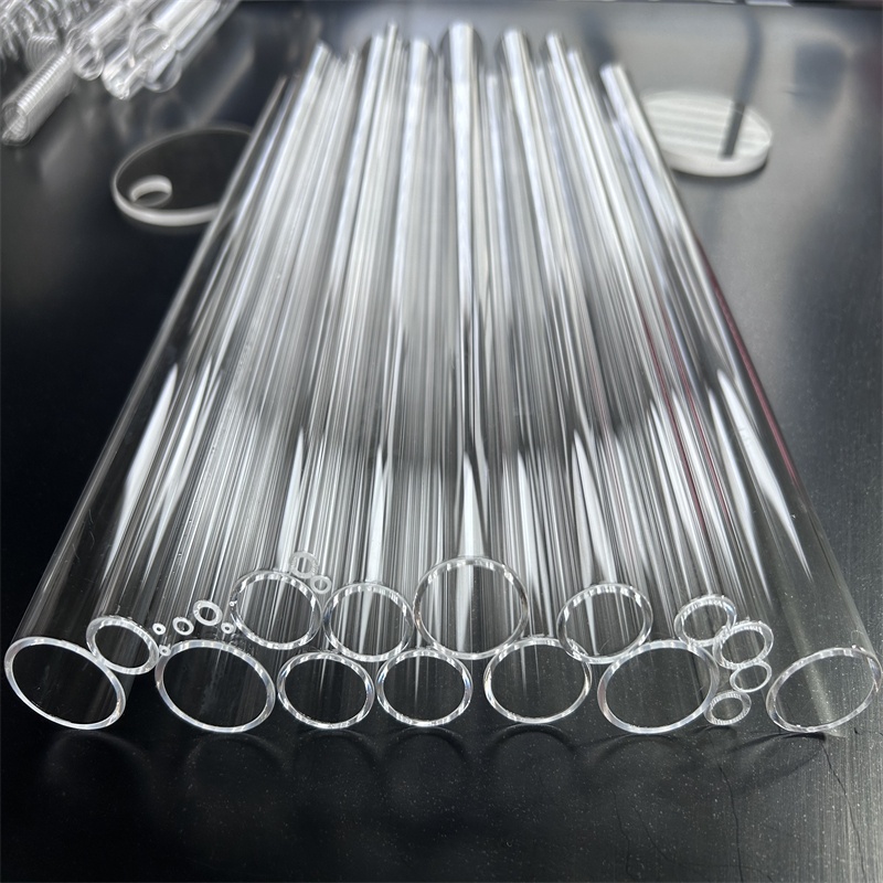
High Temperature Heat Resistant Clear 99.99% Pure Fused Quartz Twin Tube with Ozone Free Welding & Bending Services Custom Sizes
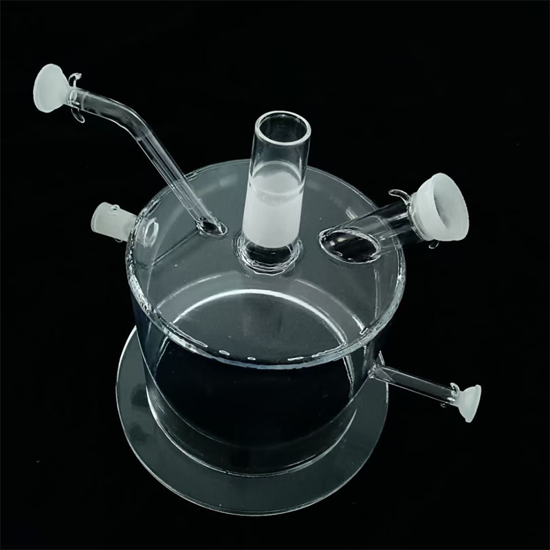
Customized High Pressure Clear Quartz Glass Tube Bending/Welding/Cutting 99.99% Pure Quartz Ozone Free Polished Surface
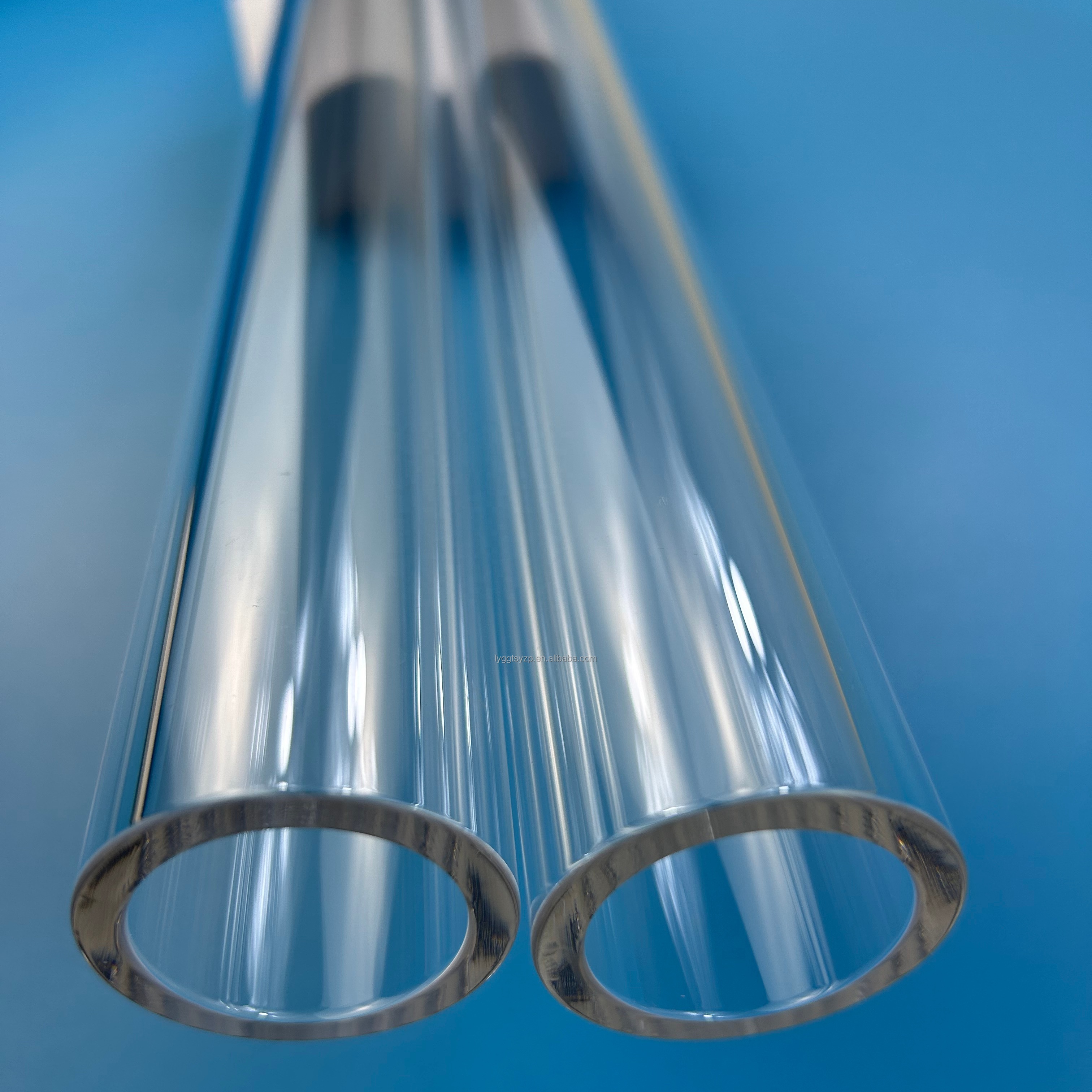
Polished Clear Quartz Twin Tube Ozone Free Heater Chemical Lab Equipment Semiconductor Furnace Tubes Welding Moulding Bending
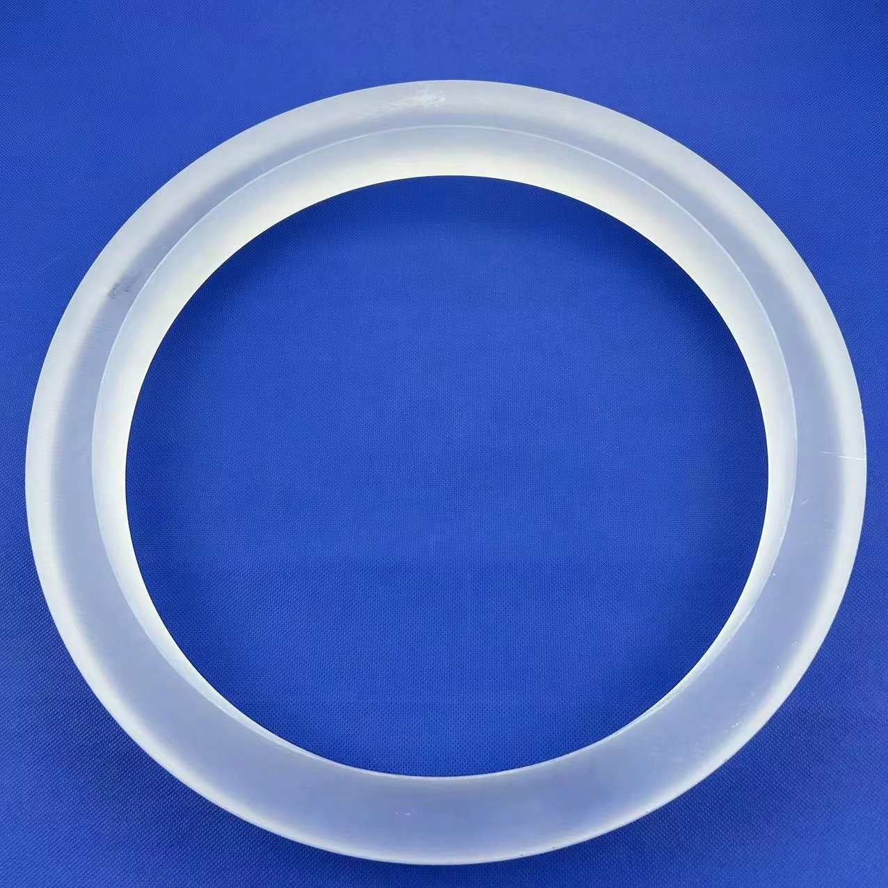
Custom Coated 99.99% Pure Quartz Rings for Semiconductor CVD Optics Applications High Pressure Moulding/Bending/Welding/Cutting
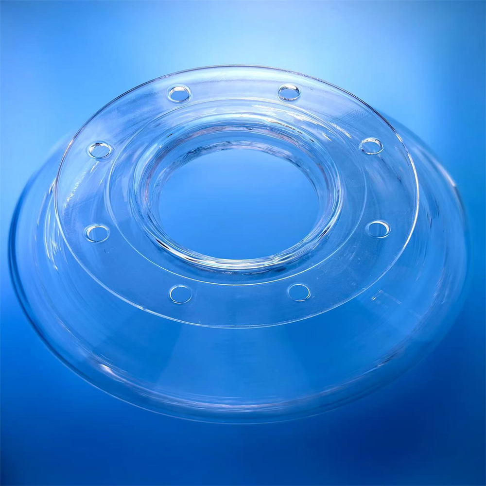
Customize Size Thickness Twin Tube Clear High Purity Flange Quartz Tube Fused Silica Polished Flange Ring Bending Welding
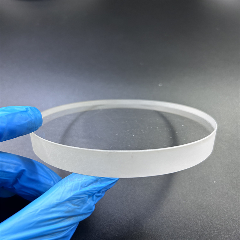
China Supplier High Temperature Transparent UV Quartz Glass Plate Polished Fused Quartz Disc Welding Cutting Optics 1100C Work
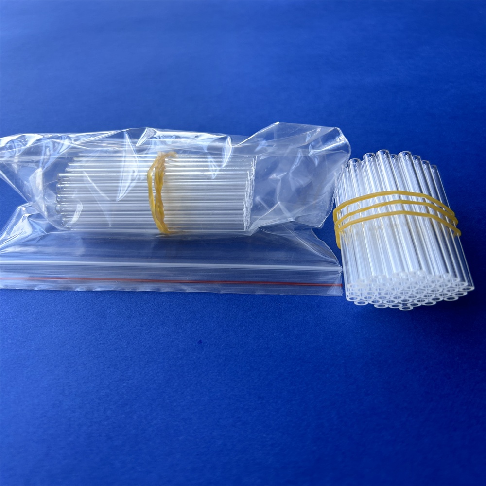
Small Diameter 0.1-20mm High Temperature Resistant 99.99% Pure Quartz Capillary Tube Cutting Bending Welding Services Ozone Free
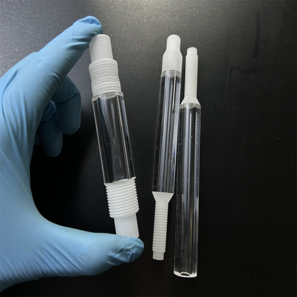
Customized High Purity Threaded Transparent UV Quartz Glass Tube with Bending Welding Cutting Moulding Services High Pressure
Fused Silica vs. Natural Fused Quartz Wafers: Metrology & Substrate Physics
A rigorous examination of optical homogeneity, bubble inclusions, hydroxyl (OH⁻) absorption dynamics, and thermal stability for cleanroom process engineers across the French microelectronics ecosystem.
| Material Metric / Physical Property | Synthetic Fused Silica (JGS1 / Suprasil Equivalent) | Optical Fused Quartz (JGS2 / Herasil Equivalent) | Infrared Fused Quartz (JGS3 / Infrasil Equivalent) | Standard Borosilicate Float Glass (Reference) |
|---|---|---|---|---|
| Chemical Purity (SiO₂ content) | ≥ 99.9999% (< 0.1 ppm metals) | ≥ 99.99% (< 20 ppm Al, Fe, Ti) | ≥ 99.995% (< 15 ppm metals) | ~ 80.5% (contains B₂O₃, Na₂O, Al₂O₃) |
| Spectral Transmission Range | 185 nm – 2,500 nm (DUV to NIR) | 220 nm – 2,500 nm (Standard Optical) | 260 nm – 3,500 nm (Extended IR) | 350 nm – 2,000 nm (Visible only) |
| Hydroxyl (OH⁻) Concentration | High (~ 800 – 1200 ppm) or Low (< 30 ppm) | 150 – 200 ppm | < 5 ppm (Water-free IR) | N/A |
| Thermal Expansion (CTE: 20°C to 300°C) | 5.5 × 10⁻⁷ / K | 5.5 × 10⁻⁷ / K | 5.4 × 10⁻⁷ / K | 32.5 × 10⁻⁷ / K (6x higher) |
| Continuous Max Operating Temperature | 1050 °C | 1150 °C | 1180 °C | 500 °C |
| Annealing Point / Softening Point | 1140 °C / 1710 °C | 1120 °C / 1683 °C | 1130 °C / 1690 °C | 560 °C / 820 °C |
| Dielectric Constant (at 1 MHz, 25°C) | 3.75 – 3.80 | 3.80 – 3.82 | 3.78 | 4.6 – 6.0 |
| Dielectric Loss Tangent (tan δ at 10 GHz) | < 0.0001 (Ultra-low RF loss) | < 0.0003 | < 0.0002 | 0.0035 – 0.0060 (High RF loss) |
| Standard Polish Roughness (Ra) | < 0.3 nm (Double-sided CMP) | < 0.5 nm (Mechanical Polish) | < 0.5 nm | > 1.0 nm |
| Refractive Index ($n_d$ at 587.6 nm) | 1.4585 | 1.4584 | 1.4586 | 1.5230 |
SEMI Dimensional Geometry
Fabricated strictly to SEMI M1 and SEMI M64 dimensional standards across all standard metric diameters: 2" (50.8mm), 3" (76.2mm), 100mm, 150mm, 200mm, and 300mm. Wafers can be specified with SEMI standard primary/secondary flats or SEMI standard edge notches for automated robotic end-effector pick-and-place tracking in automated FOUP / SMIF pods.
- Diameter Tolerance: ± 0.05 mm to ± 0.1 mm
- Thickness Options: 170 μm (cover glass), 350 μm, 500 μm, 625 μm, 725 μm, 1000 μm (± 10 μm)
- Bevel / Edge Chamfer: 45° mechanical bevel or rounded C-profile to eliminate micro-chipping
Nanoscale Topography & CMP
For anodic bonding to silicon, sub-nanometer surface smoothness is non-negotiable. Our double-sided Chemical Mechanical Polishing (CMP) utilizing colloidal ceria/silica slurry delivers pristine super-polished surfaces verified under Zygo optical interferometers and atomic force microscopy (AFM).
- Surface Roughness ($R_a$): < 0.3 nm (< 3 Å) on active faces
- Total Thickness Variation (TTV): < 2.0 μm across 100mm/150mm; < 3.0 μm across 200mm
- Bow & Warp: < 10 μm (zero residual lattice stress, annealed in vacuum)
- Surface Quality: Scratch-Dig 10-5, 20-10, or 40-20 to MIL-PRF-13830B
Laser Machining & Micro-Holes
Equipped with advanced picosecond and UV laser micro-machining centers alongside ultrasonic drilling, Zelvo delivers complex microfluidic channels, through-glass vias (TGVs), blind stepped cavities, and custom polygon geometry directly translated from French CAD/DXF specifications.
- Laser Micro-Drilling: Hole diameters down to 0.10 mm ± 0.01 mm
- Aspect Ratio: Up to 10:1 in through-hole via drilling
- Edge Chipping: Controlled strictly to < 20 μm on wafer perimeter and hole edges
- Laser Grooving: Microfluidic channel depths from 20 μm to 500 μm
High-Purity Quartz Solutions for French Innovation Clusters
From the semiconductor valleys of Isère to the aerospace corridors of Occitanie, French research and manufacturing consortia deploy our precision quartz components across demanding application scenarios.
Grenoble & Crolles: Semiconductor & 3D MEMS
Serving the vibrant microelectronics ecosystem surrounding Minatec, CEA-Leti, and industrial wafer fabs in Crolles. Fused silica wafers function as transparent temporary bonding carriers for wafer thinning, 3D TSV interconnection, and anodic silicon-to-quartz bonding in MEMS pressure transducers and inertial micro-gyroscopes.
Paris-Saclay: Photonics & Quantum Computing
Collaborating with photonics laboratories and quantum research hubs across the Plateau de Saclay and Opticsvalley. Our synthetic JGS1 substrates serve as optical window blanks, high-Q optical micro-resonators, and low-birefringence substrates for Rydberg atom traps, photonic integrated circuits (PICs), and laser diode submounts.
Toulouse: Aerospace & Defense Optics
Delivering flight-qualified, radiation-resistant fused silica substrates for CNES, Airbus Defence & Space, and Thales Alenia Space supply chains in Occitanie. Applications include solar cell cover slips, satellite optical communication crosslink mirrors, retroreflectors, and star-tracker optical windows capable of withstanding extreme cosmic thermal cycling.
Lyon & Bordeaux: Microfluidics & Bio-Photonics
Powering life science innovators, diagnostic labs, and ALPhANOV optics networks across Nouvelle-Aquitaine and the Lyon biopole. Chemically inert fused silica wafers and capillary assemblies provide background autofluorescence-free substrates for DNA microarrays, capillary electrophoresis chips, and Raman spectroscopy analytical flow cells.
The French Semiconductor Landscape Under 'France 2030' & the European Chips Act
How France's strategic push for technological sovereignty and high-yield semiconductor packaging creates demand for resilient, ultra-pure quartz manufacturing partners.
01. FD-SOI & Compound Wafer Thinning
As French chipmakers pioneer sub-20nm FD-SOI nodes and wide-bandgap Silicon Carbide (SiC) epitaxy, mechanical grinding must thin active wafers down to sub-50 μm profiles. Fused silica wafers matching exact CTE profiles serve as ultra-flat, rigid temporary bonding carriers that withstand temperatures up to 400°C during downstream chemical vapor deposition without outgassing or warping.
02. Optical Interconnects & Co-Packaged Optics
With data centers in the Île-de-France region grappling with immense power consumption from generative AI workloads, French photonics firms are actively replacing electrical copper traces with optical waveguides. Fused silica wafers offer near-zero transmission losses in the C-band (1550 nm) and low dielectric constant (ε = 3.8), creating the gold-standard platform for co-packaged optics (CPO) and silica-on-silicon interposers.
03. De-Risking Supply Chains via Direct Exporters
European supply chain disruptions have prompted French procurement directors at Tier-1 laboratories and SMEs to bypass intermediary distributors. Direct collaboration with specialized primary manufacturers like Zelvo Quartz guarantees end-to-end traceability of raw crystal sources, batch-to-batch chemical assay verification, and direct factory-level engineering reviews within 2 hours.
Why French R&D Centers & Industrial Fabs Rely on Zelvo Quartz
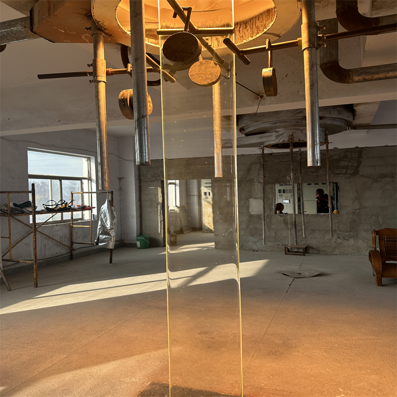
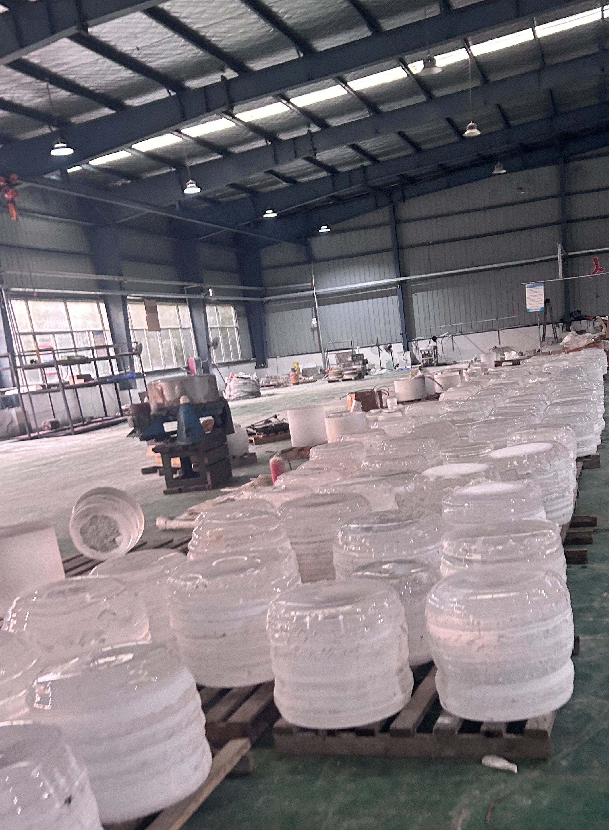
Headquartered in Donghai County—the crystal and high-purity silica capital of China—Lianyungang Zelvo Quartz Products Co., Ltd. combines premier mineral deposits with state-of-the-art precision optical machining.
99.99% Guaranteed Purity
Refined from pristine Donghai quartz deposits. Full spectrum trace-metal analysis provided per production batch ensuring zero alkali contamination in semiconductor lines.
Drawing-Based Customization
Complete in-house cold and hot processing: CNC milling, laser micro-drilling, flame bending, welding, edge profiling, and optical chemical-mechanical polishing.
Fast European Turnaround
Direct communication with veteran sales engineers. RFQ reviews within 2 hours, standard prototype dispatch in 5–7 days, and express DDP logistics directly to French facilities.
1-Piece Prototyping MOQ
Supporting university labs, research consortia, and startup pilot lines with single-piece customized wafer fabrication alongside scalable container-level capacity.
Frequently Asked Questions by French Engineering & Procurement Teams
Essential technical, regulatory, customs, and packaging answers for sourcing fused silica wafers from China to metropolitan France.
What is the difference between JGS1, JGS2, and JGS3 quartz wafer grades when ordering for a French lab?
Can Zelvo supply wafers fully compliant with SEMI standards (flats, notches, TTV, and bow)?
What Incoterms and shipping methods are used for delivery to France (Paris, Lyon, Toulouse, Grenoble)?
How are fragile quartz wafers packaged to prevent micro-scratching and particulate contamination?
Are Zelvo quartz products compliant with EU REACH and RoHS environmental directives?
What is your minimum order quantity (MOQ) and lead time for custom wafer geometries?
Accelerate Your Project with Certified High-Purity Quartz
Whether you require a single pilot fused silica wafer for university cleanroom validation or regular production batches for an industrial facility in France, our engineering team in Donghai provides rapid drawing assessments, transparent pricing, and technical support.