Micronova & Semiconductor Cleanroom Nanofabrication
Micronova, jointly run by VTT and Aalto University, houses 2,600 m2 of cleanroom space (ISO 4 to ISO 6). The fabrication of microelectromechanical systems (MEMS), silicon photonics, and compound semiconductor sensors relies critically on quartz apparatus that does not outgas or introduce metal contamination (such as Fe, Cu, or alkali ions) at elevated deposition temperatures.
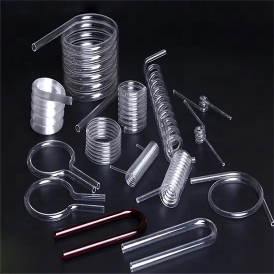
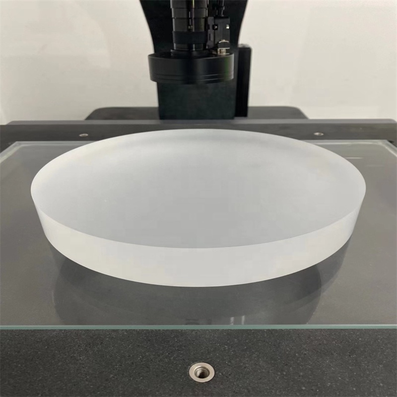
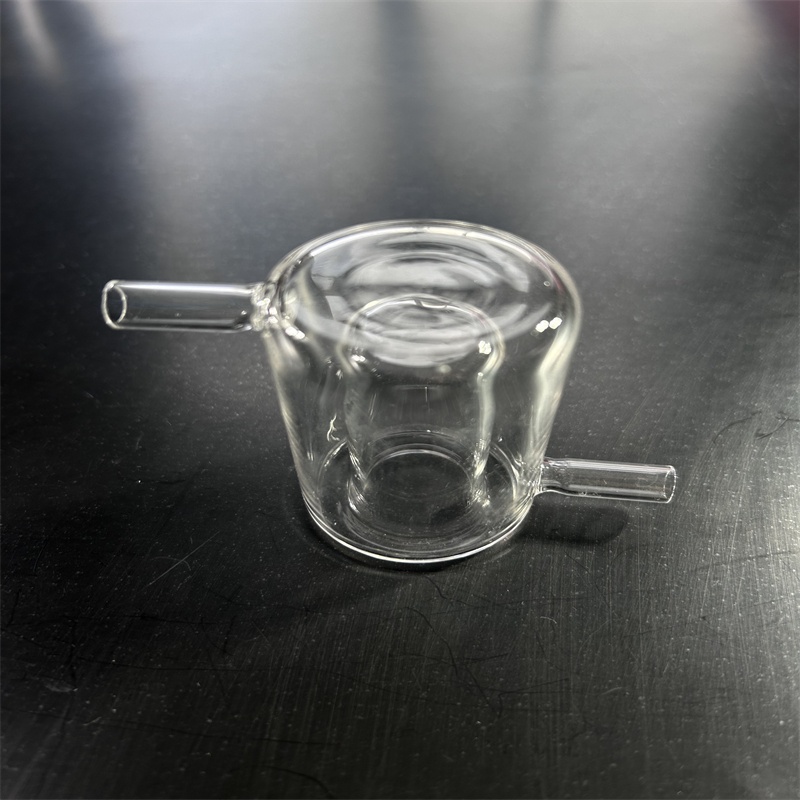
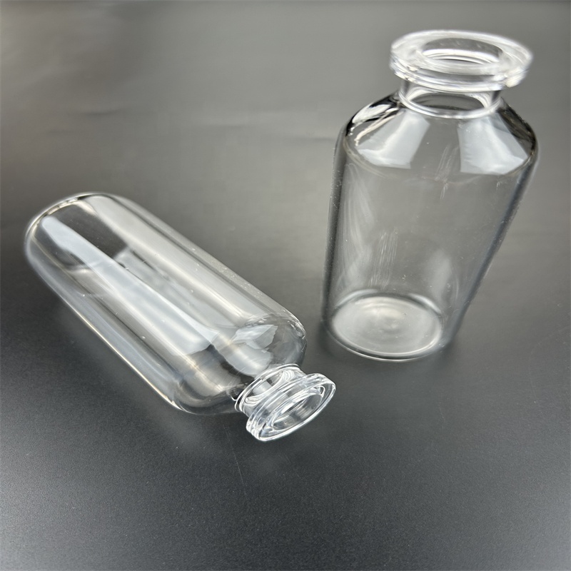
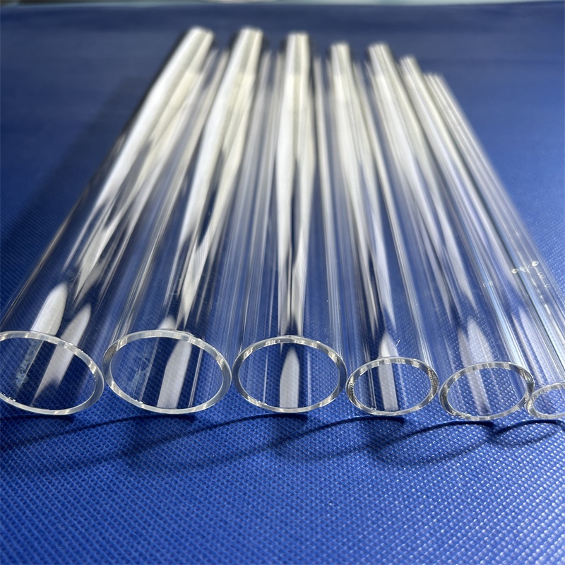
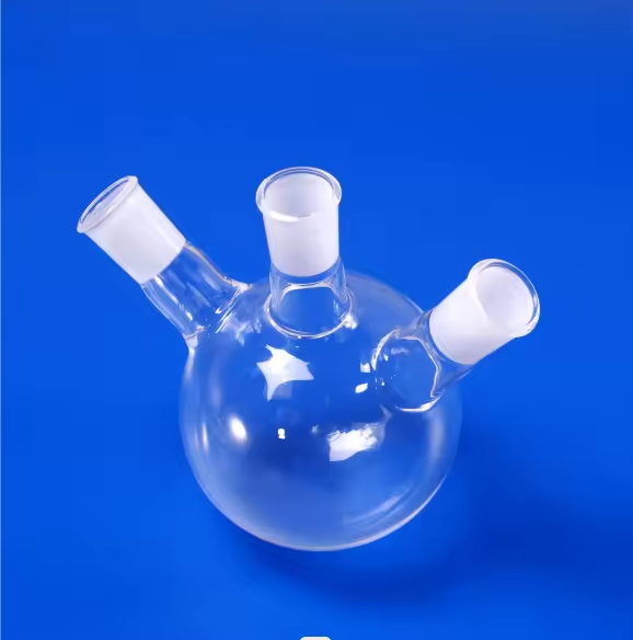
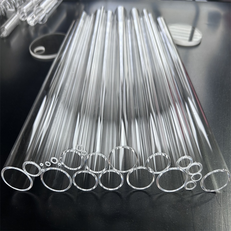
Key quartz components deployed here include custom quartz bell jars for plasma enhanced chemical vapor deposition (PECVD), furnace diffusion tubes with calibrated tolerances for ±0.5 mm thermal alignment, and low-bubble optical windows for UV lithography exposure stages.
CVD & ALD Processors
High resistance to TiCl4, TMA, and ozone flush cycles.
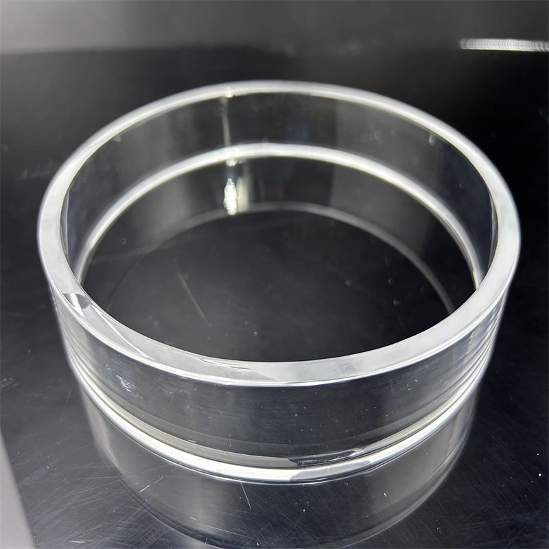
Silicon Wafer Carriers
High-temperature stability prevents wafer slippage during oxidation.